
Honway Industrial | Your exclusive polishing partner for your process
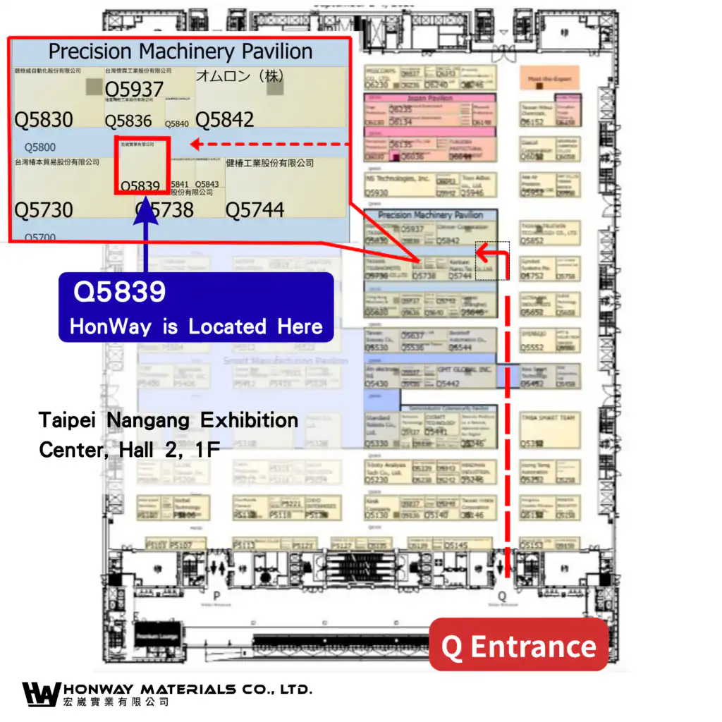
Exhibition Information:
- Dates: 09/02(Wed.)-09/03(Thr.) 10:00am-5:00pm
09/04 (Fri.)10:00am-4:00pm , 2026 - Location: 1th Floor, Hall 2, Taipei Nangang Exhibition Center
- Booth Number: N0.Q5839
Conquer the power consumption limits of next-generation AI server racks! Don’t miss the ultimate thermal solution at this year’s Semiconductor Show!
In response to the new wave of “diamond cooling” attracting global tech giants, Acer Technologies is providing comprehensive support for AI chips, from diamond wafers and diamond copper to key micro-powders, helping them overcome the thermal barriers of the liquid cooling era.
Visit our booth to see how our diamond technology perfectly matches the latest GPU architecture, unleashing peak AI computing power!
- Dates: 09/02(Wed.)-09/03(Thr.) 10:00am-5:00pm

Contact information
Telephone | Tel: +886-7-2231058 |
Exhibition time | 09/02-03 10:00am-05:00pm 09/04 10:00am-04:00pm |
Highlights of Honway Industrial Exhibition
Customized CVD Diamond Substrates/Diamond Wafers
Deploying the next-generation “diamond heatsink” technology to meet the most extreme heat dissipation and advanced packaging needs of the AI computing power era.
【Core advantages】
- Ultimate Heat Dissipation: Possesses the highest thermal conductivity among known materials, rapidly smoothing out hotspots on high-power chips.
- Absolute Insulation: Offers high electrical insulation, making it the only ultimate packaging material that can be directly bonded to bare dies and precision circuitry.
[Comprehensive Application Areas]
- AI Computing Power and Semiconductor Packaging (Market Focus Core)
- Next-Generation Diamond Cooling: Addressing the soaring power consumption of next-generation AI servers and large data centers,
- diamond substrates have become a key technology for overcoming the thermal wall in AI computing power.
- Advanced Packaging Technology: Perfectly supports 2.5D/3D stacking, HBM (High Bandwidth Memory) peripheral heat dissipation,
and serves as a heat diffusion layer for high-power transistors such as GaN (Gallium Nitride) or SiC (Silicon Carbide). - High-Frequency RF Substrates: Combining high insulation and high thermal conductivity, designed specifically for 5G/6G high-frequency communication and radio frequency (RF) components.
High-purity customized diamond micro powder
The core microparticles driving next-generation diamond heat dissipation and semiconductor precision machining: Diamond microparticles have become a key strategic material for overcoming heat dissipation bottlenecks and achieving wafer planarization (CMP) to meet the demands of AI computing power.
【Core advantages】
Extremely High Purity: Offers customized diamond micron powders with high purity, precise particle size, and high dispersibility.
Ultimate Thermal Conductivity Filler: Retains the ultimate thermal conductivity properties of diamond, making it the best inorganic filler for next-generation heat dissipation materials.
[Comprehensive Application Areas]
Advanced Semiconductor Processes
- Third-Generation Semiconductor Polishing: Ultra-precision polishing specifically designed for SiC (Silicon Carbide), GaN (Gallium Nitride), and diamond wafers.
- CMP Dressing Materials: High strength, wear-resistant, significantly extending the lifespan of semiconductor consumables.
- Next-Generation AI Thermal Insulation Materials (TIMs): Ultra-high thermal conductivity fillers blended with silicone or resin to create the ultimate heatsinks essential for high-power AI chips and data center servers.
- Precision Industry and Optics: High-end optical polishing; ultra-precision grinding of sapphire substrates, laser windows, and advanced lenses.
- Precision Tool Coating: Electroplated wear-resistant layers for micro-drills and precision tools, comprehensively doubling tool life.
Boron-Doped Diamond, BDD
The ultimate dream material that combines the characteristics of “ultra-wide heat dissipation” and “ultra-wide bandgap semiconductor”
By precisely doping the element “boron” during the CVD diamond growth process, the originally insulating diamond is transformed into a p-type semiconductor with high conductivity and an ultra-wide bandgap. It can not only dissipate heat like a diamond, but also be directly fabricated into chip components that can withstand high voltage and high frequency, making it the ultimate solution to overcome the limits of extreme environments and AI computing power.
【Core advantages】
- Integrated Conductivity and Heat Dissipation: Achieves excellent electrical conductivity while maintaining the extremely high thermal conductivity of diamond.
- Surpassing SiC/GaN: Possesses an ultra-wide bandgap and extremely high breakdown electric field, capable of withstanding extreme power densities.
- Top-Tier Electrochemical Properties: Has the widest electrochemical window known among materials, and is highly corrosion-resistant.
- Extreme Environmental Resistance: Resistant to high temperatures, radiation, and strong acids and alkalis, exhibiting long-term stability under harsh operating conditions.
[Comprehensive Application Areas]
- Next-Generation Ultra-High Power Semiconductors (AI and Electric Vehicles)
- Directly fabricate AI server power management chips and inverters that withstand ultra-high voltage and high current, reducing heat generation at the source and rapidly de-heating.
- High-Frequency High-Power RF Components (5G/6G/Satellite)
- High-frequency microwave components used in base stations and satellite communications, perfectly solving the extreme heat dissipation bottleneck under high-frequency transmission.
- Advanced Electrochemical Water Treatment (BDD Electrode)
- As the ultimate electrode material, efficiently degrades highly toxic and recalcitrant wastewater (such as PFAS and COD) from semiconductor and chemical plants.
- Bio-sensors
Combining biocompatibility and conductivity, used to manufacture high-precision, real-time electrochemical monitoring sensors within the human body.
Cu-Diamond MMC
The ultimate carrier for AI chip packaging, combining the “ultra-high thermal conductivity of diamond” and the “low expansion of metallic copper”.
In an era where AI server rack power consumption is soaring, traditional pure copper heat sinks have reached their physical limits.
【Core advantages】
- Breaking the limits of pure copper: Ultra-high thermal conductivity, instantly smoothing out localized hot spots on AI chips like a thermal sponge.
- Perfect thermal matching (low CTE): Its coefficient of thermal expansion is close to that of silicon and silicon carbide, completely solving the packaging pain points of chip warping and cracking caused by alternating hot and cold temperatures.
- Excellent processability: Retains metal processing characteristics, allowing for precision cutting, drilling, and electroplating, lowering the barrier to mass production.
- High-performance, cost-effective solution: Compared to expensive pure diamond wafers, it provides the most competitive ultimate heat dissipation solution for mass production.
[Comprehensive Application Areas]
- AI & 5G Server Heat Spreaders
- Provides a first-line heat dissipation layer for high-power GPUs and CPUs, directly bonding to the bare die to significantly reduce internal temperature rise.
- Advanced Packaging Technology (2.5D/3D Stacking)
- Serves as a high-end thermal interface carrier, providing an efficient and uniform heat dissipation path within a small, high-density integrated space.
- High-Power Radio Frequency (RF) and Laser Diodes (LDs)
- Used in GaN components and high-end lasers for 5G/6G base stations, ensuring no light decay or frequency reduction under high power.
- Electric Vehicle Power Modules (IGBT/SiC)
- Used in inverters and power modules for core power systems, improving energy conversion efficiency and ensuring reliability under extreme operating conditions.
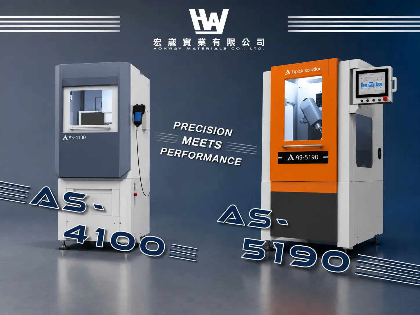
Ultra-precision polishing is the soul of the modern electronics industry. Meta Polishing models:
AS-4100, AS-5190
How important is ultra-precision polishing in manufacturing? Its applications speak for themselves: integrated circuit manufacturing, medical devices, automotive parts, digital accessories, precision molds, various bearings, and aerospace equipment.
As a highly demanding process, ultra-precision polishing requires both equipment and materials (polishing fluid); neither can be dispensed with.
【Core advantages】
- Enables ultra-precision polishing of free-form surfaces.
- The surface remains scratch-free even under 100x microscopy.
- Effectively reduces surface roughness and controls Ra value.
- Effectively reduces waviness Wa.
- Precisely maintains excellent workpiece profile after polishing.
- Suitable for various materials, such as: electroless nickel, copper, aluminum, tungsten steel, and mold steel.

Ultra-finishing solutions: the key to achieving nano-level precision
In response to the stringent demands for polishing workpieces such as difficult-to-grind materials and super-hard metals, Honway provides grinding and polishing consumables and processing equipment designed specifically for them.
We are well aware of the manufacturing challenges these materials present. Through precise formulation and equipment design, we can help you reduce processing time, overcome surface defects, achieve the nano-level surface finish and flatness required for components, and comprehensively improve product performance and yield.
Do you have these problems? HonWay provides solutions!
Honway Solution: Our diamond abrasive tools can be designed with proportions adjusted according to needs, specifically for fine, controlled cutting, avoiding micro-cracks and edge chipping, and ensuring stable surface flatness and roughness.
Honway Solution: Our customized polishing formulas and professional technical support can accurately analyze and resolve surface defects caused by consumables, significantly improving product yield.
Honway’s solution: Through innovative grinding and polishing consumables and optimized process recommendations, we help you shorten polishing time, significantly improve production efficiency, and reduce single-wafer costs.
Honway’s solution: Acer offers competitive pricing while ensuring superior quality, giving you a better total cost of ownership (TCO).
Honway’s solution: Our company’s diamond grinding tools have extremely high hardness and wear resistance, which can greatly improve the cutting rate and processing efficiency, and shorten the processing time.
Technology Insights / Industry Views
1+N Metallographic Magnetic Fixation System: 3-Second Disc Change Specimen Preparation Guide
Decoding Metallographic Grinding Disc Ra Performance: Electroplated, Honeycomb, and Resinoid Specimen Preparation Guide
In-Line Truing and Dressing of Vitrified Bond Mounted Points: The Holy Grail of Automated Mass Production
Electroplated Diamond Mounted Points Maintenance: Maximizing Single-Layer Grit Life and High-Speed Parameter Tuning
Breaking Micron Processing Limits: How 1mm Ultra-Thin Diamond Files Resolve Rib and Narrow Slot Grinding Pain Points
How to Prevent Thermal Cracking in Precision Mold Finishing: A Benchmarking Guide to Non-Annealing Grinding Process Workflows
Diamond Nylon Brush: The Advanced Cross-Hole Deburring & Chamfering Guide
Contact Information and Map
|
Telephone |
Tel: +886-7-2231058 |
|
|
|
|
Exhibition time |
09/02-03 10:00am-05:00pm 09/04 10:00am-04:00pm |
Facebook
Threads
LinkedIn
Email