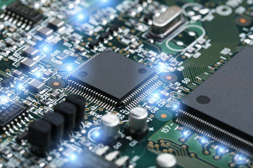
In modern fiber optic component manufacturing, hard disk drive (HDD) magnetic head fabrication, and advanced semiconductor failure analysis (FA) laboratories, conventional polishing cloths paired with loose abrasive slurries often introduce a critical geometric flaw: “edge roll-off.” When processing materials of extreme hardness or complex, multi-layered brittle matrices, achieving absolute coplanar flatness requires a high-rigidity polyester substrate support.
In this engineering brief, the Honway technical team decodes the underlying material science of Diamond and Alumina PE Lapping Films. Discover how micro- and nano-scale precision coating technologies enable process engineers to overcome strict geometric tolerances in ceramic ferrule and magnetic head manufacturing, while mitigating scratching and adhesive residue defects across high-throughput production lines.
📋 Table of Contents
- 1. Technical Advantages: Micro/Nano-Scale Coating for Sub-Micron Surface Roughness
- 2. Core Selection Matrix: HW-261X vs. HW-661X Formulations
- 3. Operational Workflow Efficiency: High-Performance PSA Backing Systems
- 4. Field Proven Diagnostics: Applications in Hard-Brittle Processing and Failure Analysis
- 5. Engineering FAQ: Resolving Common Lapping Film Technical Bottlenecks
- 6. Knowledge Base: Advanced Surface Finishing and Consumable Integration
- 7. Procurement Directory & Corporate B2B Inquiry Channel
1. Technical Advantages: Micro/Nano-Scale Coating for Sub-Micron Surface Roughness
Precision lapping film differentiates itself from standard waterproof sandpapers through its structural substrate boundaries and tight abrasive particle sorting tolerances. Honway’s PE films utilize a high-modulus, high-tensile polyester backing that guarantees absolute cross-sectional thickness uniformity.
Leveraging advanced precision slurry-coating processes, precisely sized micro- and nano-scale abrasive minerals are bonded securely to the polyester surface with a highly uniform spatial density. This structural composition delivers two significant processing advantages:
- 💎 Absolute Geometric Coplanarity: Because the high-rigidity PE backing material resists elastic compression under heavy downward polishing pressures (unlike compliant fabric polishing cloths), it maintains a rigid cutting profile. This mechanics completely eliminates edge rounding and perimeter roll-off variations, making it the industry-recognized wafer edge roll-off mitigation solution.
- 💎 Superior Surface Finish Control ($R_a$ Performance): From micro-scale coarse leveling to nano-scale mirror finishing, the uniform orientation of the secured abrasive grain ensures consistent material removal rates (MRR). It eliminates loose macro-particles from causing stray superficial micro-scratches, allowing production surfaces to predictably reach extreme specular mirror clarity.
2. Core Selection Matrix: HW-261X vs. HW-661X Formulations
To address varying material configurations and multi-stage sequential polishing cycles, Honway engineers have developed two flagship product series. Procurement managers and line engineers can review the following formulation specifications, or jump directly to our master directory: 【Honway High-Precision Polishing Film Catalog】.
A. HW-261X Series: High-Purity Alumina ($\text{Al}_2\text{O}_3$) Precision Film
- Mineral Formulation: High-purity, synthetic aluminum oxide ($\text{Al}_2\text{O}_3$).
- Microstructural Characteristics: The alumina crystals feature optimized friability. Under sustained processing pressure, the grains undergo micro-fracturing to continuously expose fresh, razor-sharp cutting facets (self-sharpening action). This delivers a highly controlled, non-aggressive abrasive force.
- Primary Applications: Final polishing of fiber optic connector zirconia/glass ceramic ferrule end-faces, HDD magnetic head air-bearing surface (ABS) corrections, and precision leveling of non-ferrous metals (Copper, Aluminum) and carbon steels.
B. HW-661X Series: Superabrasive Diamond High-Precision Film
- Mineral Formulation: Monocrystalline or polycrystalline premium diamond micro-powder.
- Microstructural Characteristics: Diamond exhibits unmatched crystalline hardness and wear resistance. This enables positive, forced micro-cutting action against high-hardness substrates, ensuring long-term cutting efficiency and extended film service life without structural degradation.
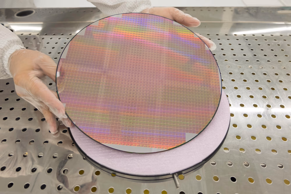
- Primary Applications: High-hardness and brittle compound configurations, including tungsten carbide tooling dies, sapphire wafer substrates, industrial ceramic components, and wide-bandgap third-generation semiconductor (SiC / GaN) wafer planarity tuning.
- Direct Product Interface: 👉 Access Honway HW-661X Diamond Film / Diamond PE Film Specifications & Sample Orders
3. Operational Workflow Efficiency: High-Performance PSA Backing Systems
In high-volume manufacturing environments and advanced material analysis laboratories, minimizing consumable swap changeover times (downtime) directly impacts processing margins. Traditional non-adhesive lapping films require auxiliary mechanical clamps or secondary spray adhesives, which frequently introduce trapped air pockets, surface ripples, and difficult cleaning cycles.
Honway’s complete lapping film lineup features an optional, engineered PSA (Pressure Sensitive Adhesive) backing configuration:
- ⏱️ Three-Second Application: Technicians simply peel away the low-energy release liner and apply the film directly onto a ground glass or metallic backing platen. The adhesive generates high shear resistance instantly, preventing displacement or edge lifting under high-RPM rotation and continuous coolant fluid flow.
- ⏱️ Clean-Peel, Zero-Residue Technology: The modified PSA layer is applied at a micron-scale thickness to protect the base PE film’s parallel planarity. Upon exhaustion, the film peels cleanly away from the platen as a singular cohesive sheet, leaving zero adhesive residues behind and eliminating time-consuming chemical cleanup operations.
💡 Visual Calibration Note: Honway’s complete lapping film series utilizes a strict color-coded system corresponding to specific micron and sub-micron grit sizes, entirely removing the risk of cross-contamination or grit mixing on the processing floor.
4. Field Proven Diagnostics: Applications in Hard-Brittle Processing and Failure Analysis
By enforcing a flat, high-modulus cutting interface, Honway Diamond and Alumina films successfully isolate and correct geometric deviations. The following matrix details field deployment benchmarks across three primary high-tech sectors:
| Target Application | Processing Challenges & Engineering Solutions | Recommended Grade & Sizing |
|---|---|---|
| Fiber Optic Telecommunications | Resolving Differential Material Erosion: The silica core and zirconia ferrule possess vastly distinct hardness coefficients. Standard abrasive pads generate center pitting. Honway Alumina films maintain co-planar erosion rates, ensuring scratch-free PC/APC spherical end-faces with certified insertion/return loss metrics. | HW-261X Series (0.1μm to 1μm Final Polish) |
| HDD Magnetic Components (GMR / TMR Heads) |
Sub-Nanometer Controlled Stripping: Giant Magnetoresistive heads are composed of ultra-thin, multi-layered metal-ceramic stacks. Honway lapping films provide low, stable nano-scale material removal depth control, preventing interlayer smearing or micro-fracturing to retain magnetic read-write yields. | HW-261X / HW-661X Sequential Grit Escalation |
| Advanced Substrates (SiC / GaN / Sapphire) |
Forced Machining of Hard-Brittle Wafers: Materials with a Mohs hardness ≥ 9 resist standard silicon carbide sheets entirely. Honway’s fixed diamond micro-grains perform precise mechanical micro-machining and surface leveling, rapidly thinning the workpiece and cutting subsequent CMP chemical-mechanical polishing cycles in half. | HW-661X Diamond Series (3μm to 30μm Grinding/Lapping) |
5. Engineering FAQ: Resolving Common Lapping Film Technical Bottlenecks
Honway’s Material Analysis (MA) desk has compiled the most critical diagnostic inquiries from optical and semiconductor processing floors regarding grit sequence selection and residue management:
Q1: During multi-stage fiber optic ferrule finishing, what are the precise sequencing rules for film grit sizes? What happens if a step is omitted?
Engineering Analysis: High-precision optical polishing is a rigid, multi-stage progressive sequence that must strictly advance from coarse to sub-micron sizing. A typical standard workflow utilizes a 9μm or 5μm diamond lapping film for initial epoxy de-reeling and ceramic leveling; followed by a 1μm or 0.5μm alumina film to refine and overwrite the preceding macro-scratch profiles; and concludes with a 0.1μm fine silica or alumina layer for the final specular finish.
If an engineer skips a sequence step (e.g., executing a direct transition from 9μm down to 0.5μm), the ultra-fine abrasive minerals will lack the required depth of cut to flatten the deep macro-grooves left by the 9μm step. While the surface may appear shiny, sub-surface macro-scratches remain embedded within the optical path, generating signal scattering and severe return loss failures during optoelectronic testing.
Q2: Our current lapping film leaves a highly persistent adhesive film on the master glass platens after stripping. How should we handle this residue buildup, and how does Honway resolve this?
Engineering Analysis: Platen adhesive contamination is a widespread operational bottleneck. Low-grade pressure-sensitive adhesives often degrade when exposed to frictional heat, coolant additives, and chemical surfactants, causing the polymer matrix to shear and cross-link directly onto the glass or metallic master plate. Technicians are then forced to manually scrape the platens using solvents like petroleum spirits or isopropyl alcohol (IPA), risking physical scratches that ruin the master platen’s reference flatness.
Honway addresses this through high-cohesion chemical cross-linking modifications within our PSA formulation. Our adhesive matrix is specifically optimized for high thermal stability, moisture isolation, and elevated shear modulus. Upon depletion, the adhesive boundary peels away cleanly along with the polyester backing sheet, leaving zero residue on the platen surface and completely eliminating solvent-scrubbing steps from your operational maintenance routine.
6. Knowledge Base: Advanced Surface Finishing and Consumable Integration
To maximize the operational yield of high-rigidity lapping film systems, process controls must align with correct down-stream polishing consumables and calibrated metrology standards. We invite you to explore our technical insight columns:
- 📊 Surface Roughness Metrology: Grinding, Polishing, and Surface Roughness Comparison Chart: Querying Industrial Mesh Size and Ra/Ry/Rz Data
- 🧲 Laboratory Automation Retrofits: Metallographic Magnetic Fixation System 1+N Transition Guide: Achieve 3-Second Disc Changes and Eliminate Mechanical Clamping Rings
- 🔬 Abrasive Carrier Mechanics: Decoding Metallographic Grinding Disc Ra Performance: Electroplated, Honeycomb, and Resinoid Structural Variations
- 👉 Optical & Glass Restorations: Cerium Oxide Polishing Powder & Slurry: Industrial Glass Scratch Repair and Optical Surface Restoration Guide
7. Procurement Directory & Corporate B2B Inquiry Channel
Whether you are managing a high-throughput fiber optic patch-cord assembly facility or an advanced wafer level failure analysis laboratory, Honway’s micro-coated Diamond and Alumina Lapping Films deliver the geometric repeatability required to secure your product line yields.
🚀 Optimize Your Process Line: Request Honway Lapping Film Technical Samples & Bulk Quotations Today!
Honway provides specialized corporate B2B procurement pipelines and technical adaptation consulting:
- 🛒 Direct Specifications Submission: Navigate to the 【Honway High-Precision Polishing Film Sourcing Section】 to transmit your exact dimension and micron requirements.
- 👨🔬 Application Engineering Consultation: To address precise wafer edge roll-off challenges, provide your substrate composition, targeted $R_a$ thresholds, and equipment specifications to our desk for custom grit sequence mapping.
Verified Honway Product Portfolios for Global Inquiries & Sample Orders
Browse our verified online catalog below to order sample quantities directly with premium worldwide shipping logistics, or connect with our customer success desk for contract bulk pricing arrangements.
- Master Directory: High-Precision Polishing Film Classification Index
- Diamond PE Film Landing Page: HW-661X Diamond Film / Diamond PE Film Dedicated Product Page
- Magnetic Core Base Platens: Honway Magnetic Disc Specifications Page
- Teflon Protective Barriers: Honway Teflon Anti-Stick Disk Integration Interface
- Coarse Stage Carrier (Electroformed): Honway Rigid Electroplated Diamond Platens
- Fine Stage Carrier (Honeycomb SiC): HW-SiC-I Triangular Honeycomb Abrasive Discs
- Fine Stage Carrier (Honeycomb Alumina): HW-Al-I Micro-Powder Alumina Finishing Discs
- Superabrasive Carrier (Honeycomb Diamond): HW-Primo Diamond High-Hardness Composite Discs
Honway Customer Success Office (Taiwan Headquarters HQ)
· 📨 Corporate RFQ Inquiries: Click to immediately route to 【Contact the Honway Technical Projects Team】. Specify desired model codes (HW-261X / HW-661X) and targeted micrometer profiles. Our desk will assign a technical account manager within 24 business hours.
· 📞 International Hotline: +886 7 223 1058 (Monday – Friday, 09:00 – 18:00, GMT+8)
· 📱 Official Communications Channel: Access the Honway Group Corporate Facebook Feed for direct product engineering messaging.