In advanced semiconductor fabrication and high-end component manufacturing, working with diverse substrates like compound semiconductors (GaAs Gallium Arsenide / InP Indium Phosphide), precision optical glass, and hard-brittle technical ceramics presents steep finishing challenges. Selecting the correct combination of polishing consumables—including grinding mounted points, polishing pads, chemical slurries, and oil stones—is the defining factor that dictates your plant’s Material Removal Rate (MRR) and final surface roughness (Ra) targets. To streamline your engineering layout, the application engineering group at HonWay Materials has compiled this comprehensive, one-stop reference guide to accelerate your production line optimization.
Table of Contents
- 1. Overcoming Core Technical Bottlenecks in Hard and Brittle Material Finishing
- 2. HonWay Consolidated Matrix: High-End Polishing Consumables Configuration Reference Table
- 3. Toolroom Troubleshooting FAQ: Advanced Operational and Parameter Adjustment Strategies
- 4. Strategic Procurement: Securing Scalable Supply Chain and Technical Integration Support
1. Overcoming Core Technical Bottlenecks in Hard and Brittle Material Finishing
Whether managing an optoelectronics facility, an RF chip foundry, or a precision optical lens manufacturing plant, process engineers running hard-brittle substrates regularly bump into severe structural and surface quality thresholds:
- ❌ Improper GaAs Consumable Matching: Compound semiconductors exhibit incredibly low fracture toughness. If the polishing pad stiffness or operational downforce parameters are mismatched, it triggers microscopic sub-surface cracks, edge roll-off, or catastrophic wafer edge chipping.
- ❌ Inefficient Silicon Carbide Ceramic Grinding Wheel Throughput: When facing high-hardness industrial technical ceramics (such as SiC or Al2O3), conventional abrasives degrade and glaze over rapidly. This results in sluggish material removal rates, prolonged cycle times, and budget overruns.
- ❌ Yield Failure from Micro-Scratches: During final-stage fine polishing, any sub-optimal abrasive particle distribution leads to micro-agglomeration. This inflicts irreversible surface scratches, forcing engineers to scrap high-value wafers or optical lenses.
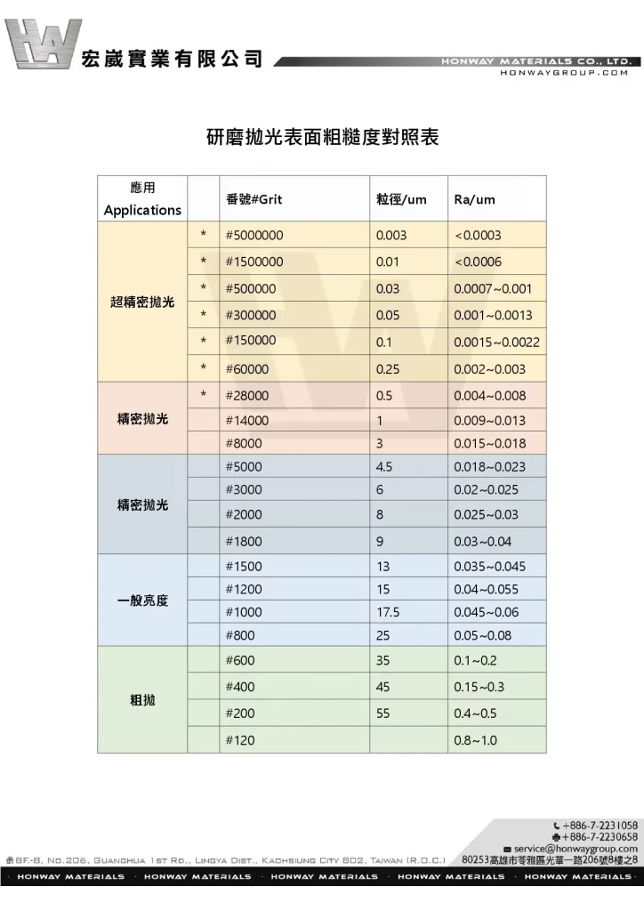
2. HonWay Consolidated Matrix: High-End Polishing Consumables Configuration Reference Table
B2B research directors and production managers require data-driven, empirical criteria to balance yield with operating costs. The configuration matrix below represents HonWay’s engineered standard for compound substrates, providing a stable baseline for your polishing line setup:
| Target Substrate Material | Recommended Abrasive Wheel / Pre-Polishing Tool | Recommended Polishing Pad Architecture | Recommended Slurry / Fluid Abrasive Media |
|---|---|---|---|
| Compound Semiconductors (GaAs, InP) |
Micron-grade fine grit Electroforming Diamond/CBN Internal Points / Diamond and Boron Nitride Grinding Wheel | Soft polyurethane-impregnated non-woven polishing pads (HonWay Metallographic Polishing Pads FS-08 Series) |
High-purity colloidal silica slurry / Diamond Liquid Grinding Solution |
| Precision Optical Glass (Quartz, Sapphire Substrates) |
Diamond Fiber Oil Stone (for heavy scale purging) / Diamond Handmade File | Vertical through-hole macro-porous coated polishing pads (HonWay Metallographic Polishing Pads FS-12 / FS-16) |
Cerium Oxide Polishing Powder / Alumina Polishing Solution |
| Industrial & Electronic Ceramics (SiC, Al2O3) |
High-rigidity Diamond and Boron Nitride Grinding Wheel / EDM-targeted EDM & DF Oil Stones | Hard, high-modulus coated composite polishing pads (for strict local planarization) | High-concentration polycrystalline diamond slurry / High-purity finishing fluid |
💡 System Procurement Note: To request technical spec sheets, evaluate specific physical cross-sections, or request volume testing samples for factory deployment, please reach out directly to our application desk.
3. Toolroom Troubleshooting FAQ: Advanced Operational and Parameter Adjustment Strategies
Q1: When executing Gallium Arsenide wafer polishing, what are the root causes of wafer fracture, and how can we mitigate subsurface stress?
【Expert Insight】 The lattice structure of GaAs is exceptionally fragile. When investigating GaAs wafer crack prevention, structural failure almost always traces back to excessive mechanical shear or sudden downforce spiking. To resolve this, engineers should configure a low-downforce, high-velocity parameter matrix.
Regarding consumables matching, it is mandatory to use a high-compressibility, polyurethane-impregnated non-woven pad (such as HonWay Metallographic Polishing Pads FS-08) that can dynamically conform to the wafer’s macro-topography. This must be paired with a gentle compound semiconductor chemical fluid like a high-purity colloidal silica slurry. This balanced Chemical Mechanical Planarization (CMP) profile prioritizes chemical surface softening over aggressive physical abrasion, reducing subsurface stress and edge-chipping metrics to near zero.
Q2: What is the processing bottleneck when finishing precision quartz components, and how do we ensure quartz glass scratch elimination?
【Expert Insight】 Achieving consistent quartz glass scratch elimination depends completely on securing unhindered swarf evacuation channels. Grinding hard, brittle optical silica produces a massive volume of microscopic glass swarf. If these fine particles stagnate under the polishing pad, they quickly agglomerate into coarse clusters that score deep, permanent scratches across the component surface.
The solution requires replacing solid-faced pads with custom coated configurations featuring vertical straight through-holes (such as HonWay Metallographic Polishing Pads FS-12/16) or engineered concentric grooves. This geometry utilizes fluid dynamics to continuously flush spent swarf and heat out of the cutting zone, ensuring fresh, unpolluted chemistry interacts with the quartz glass, eliminating micro-scratching phenomena entirely.
🔗 Cross-Process Technical Reading: Deepening Your Surface Engineering Knowledge
To master the underlying chemical and physical interactions governing high-end finishing consumables, consult our engineering group’s specialized technical guides:
- 👉 HonWay Guide: Match Polishing Slurries for Semiconductor, Metal & Ceramic Substrates
- 👉 Impregnated vs. Coated Polishing Pads: Microstructural Engineering for Sapphire & Quartz CMP
- 👉 Revolutionary Tech in Polishing: The Ultimate Selection Guide for Polycrystalline V.S. Monocrystalline Diamonds
- 📋 Rigorous Inventory Control and Batch-to-Batch Consistency: From Electroforming Diamond/CBN Internal Points and engineered Diamond Fiber Oil Stones to the entire Metallographic Polishing Pads lineup, our warehouse maintains robust stock counts to protect your high-volume manufacturing schedules.
- 👨🔬 Custom Process Integration and Parameter Calibration: Our field application engineers are trained to analyze your current toolroom machinery capabilities—evaluating exact spindle speeds, pressure capabilities, and flow delivery systems—to design a custom, substrate-matched consumable toolkit.
Take Action: Reach out to HonWay Materials’ customer success division today to obtain your dedicated semiconductor and advanced substrate consumable quotation package.
Request Technical Consumables Samples & B2B Process Consultation Here
HonWay Customer Success Office (Taiwan HQ)
Company Name: HonWay Materials Co., Ltd.
Official B2B Inquiry Email: [email protected]
Business Hours: Monday – Friday, 09:00 – 18:00 (GMT+8)
International Direct Line: +886 7 223 1058
Official Social Channels: Honway Group Facebook | LinkedIn Corporate Page