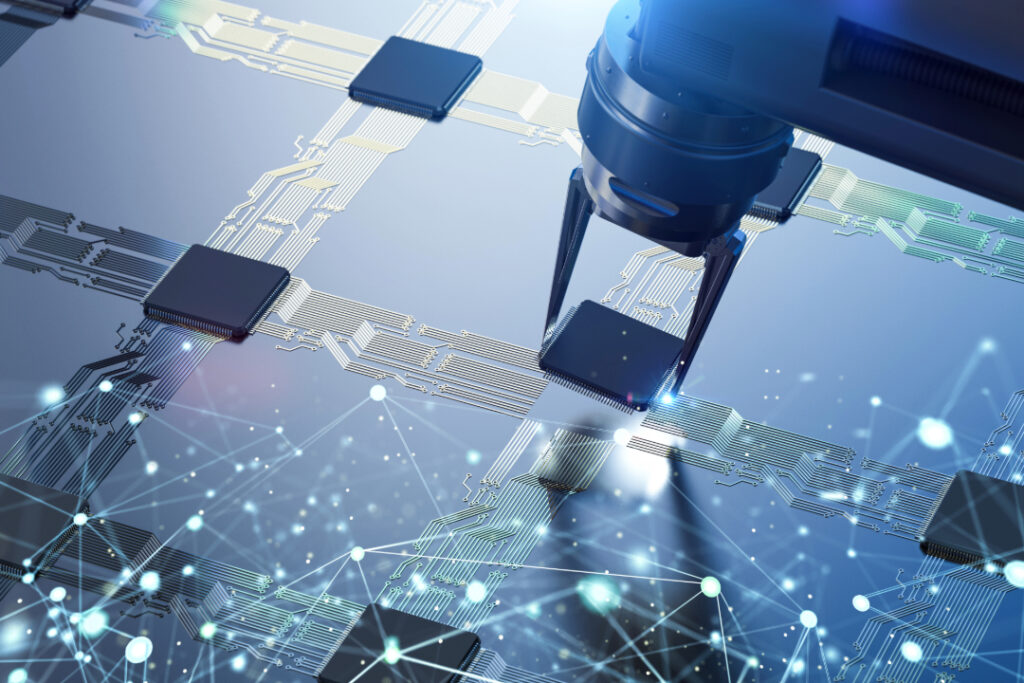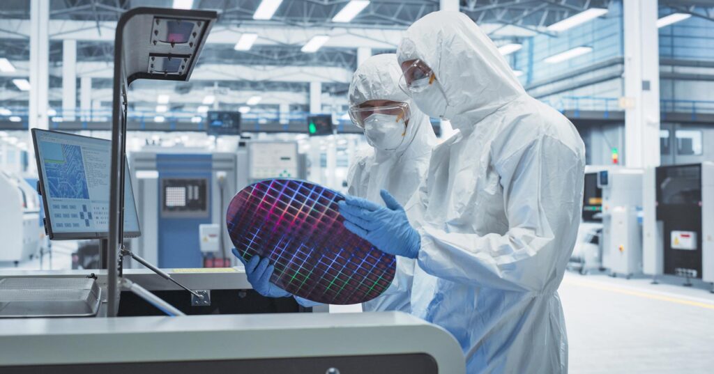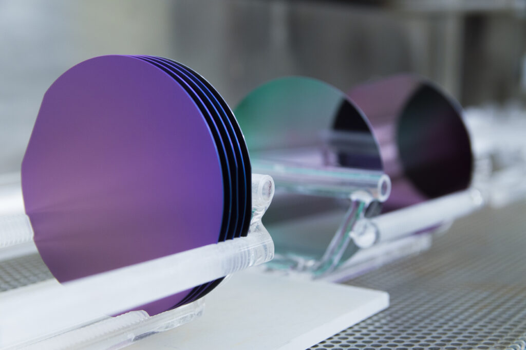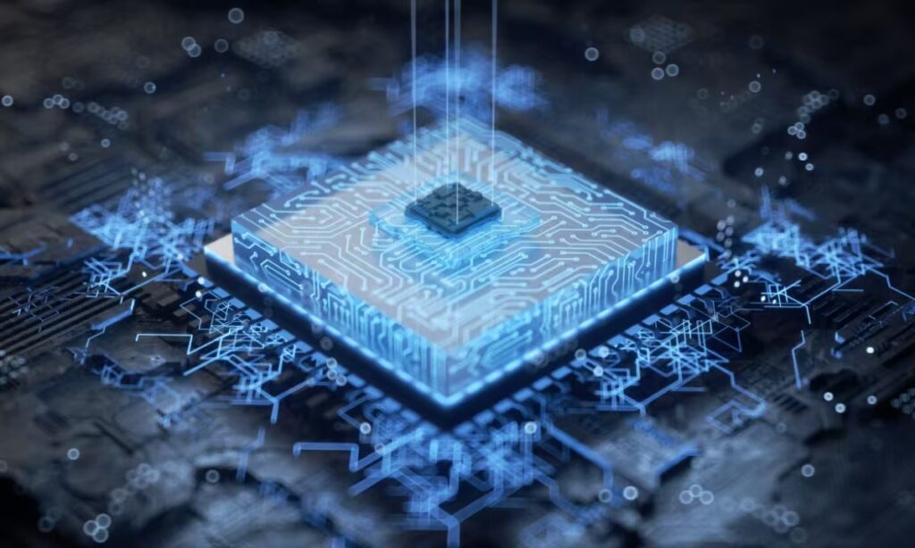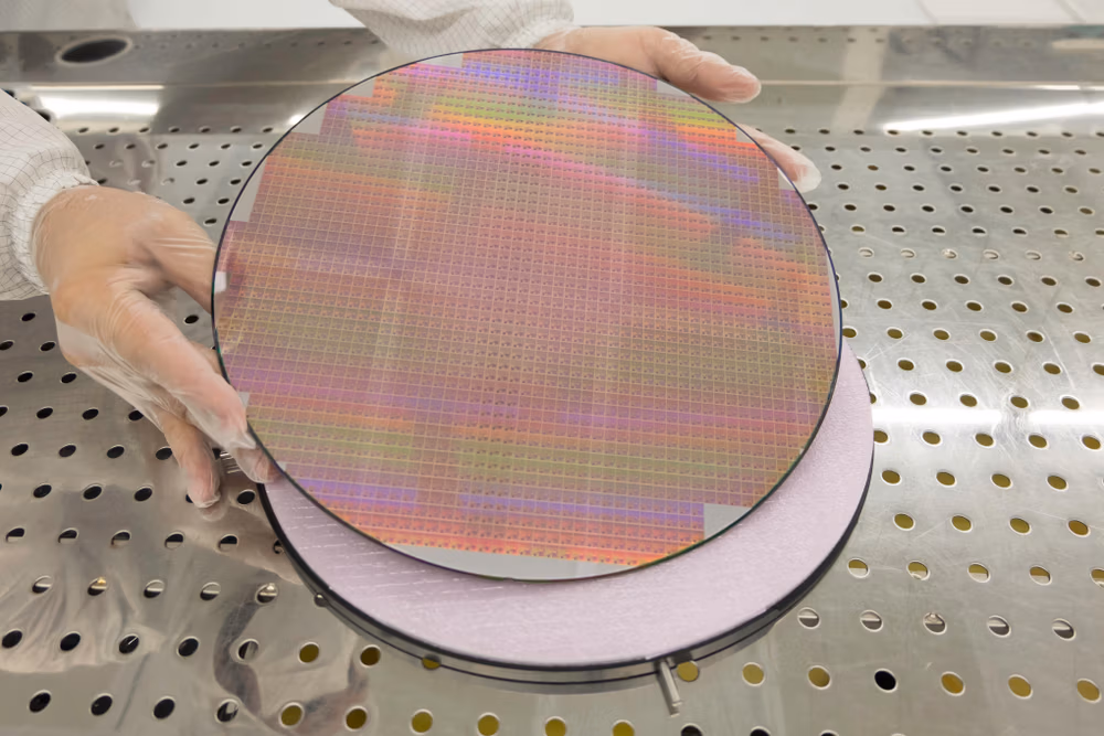
Semiconductor grinding and polishing technology
In semiconductor manufacturing, grinding and polishing are key processes to ensure that the wafer surface achieves extreme flatness and defect-free mirror finish. Grinding is responsible for precisely controlling wafer thickness and removing rough surfaces, while polishing achieves nanometer-level flatness through technologies such as chemical mechanical polishing (CMP). Both are critical to the performance of integrated circuits. Honway will deeply explore the various technologies, challenges, and latest developments in semiconductor grinding and polishing to help you master the secrets of wafer surface treatment.