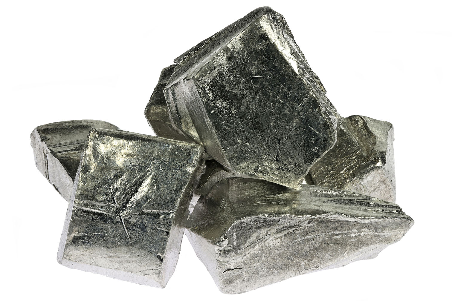
In the modern high-tech industry, the manufacturing of many key components relies on rare metals, and Indium (In) is an indispensable member among them. Indium is a soft, silvery-white, highly ductile metal. Due to its excellent conductivity, optical properties, and chemical stability, it is widely used in semiconductors, solar cells, displays, and aerospace fields. This article will comprehensively analyze this rare metal, known as the “Golden Supporting Actor of the Electronics Industry,” covering its historical origins, basic introduction, physical and chemical properties, purity specifications, and applications.
Table of Contents
Historical Origins
Indium was discovered in 1863 by German chemists **Ferdinand Reich** and **Hieronymus Richter** during ore experiments in Freiberg, Saxony. At the time, they were studying ores containing thallium but unexpectedly observed a bright indigo blue line in the spectrum. This unique spectral signal proved the existence of a new element. Due to this blue spectral characteristic, scientists named it “Indium,” derived from the Latin word *indicum*, meaning “indigo blue.”
In 1864, Richter successfully isolated metallic indium and exhibited the first indium ingot weighing 0.5 kg at the 1867 Paris World Expo, marking the birth of indium and the beginning of its industrial application.
Basic Introduction to Indium
- Chemical Symbol: In
- Atomic Number: 49
- Atomic Weight: 114.818
- Classification: Post-transition metal, Boron group
- Crustal Abundance: Approx. 0.21 ppm, classified as a rare element
- Appearance: Silvery-white, soft with metallic luster, similar to tin
Indium mainly exists in sphalerite and is usually extracted as a by-product of zinc refining. Due to its extremely low abundance in nature, its supply is highly dependent on the zinc mining industry.
Physical and Chemical Properties
Physical Properties
- Atomic Weight: 114.818
- Density: 7.30 g/cm³
- Melting Point: 156.61 °C
- Boiling Point: 2060 °C
- Hardness: Mohs 1.2, extremely soft; can be scratched with a knife or leave a mark on paper
- Structure: Body-centered tetragonal
- Special Properties:
- Becomes a superconductor below 3.41 K
- Excellent ductility and wettability (adhesion)
- Emits a high-pitched “indium cry” when bent
Chemical Properties
Indium’s chemical properties lie between Gallium (Ga) and Thallium (Tl), allowing it to bond tightly with materials like glass, quartz, and mica. It forms various compounds such as Indium Oxide (In₂O₃), Indium Chloride (InCl₃), and Indium Sulfide (In₂S₃), which are widely used in electronics, optoelectronics, and optical fields.
Purity and Specifications of Indium
Applications of Indium require extremely high purity. Common specifications are as follows:
| Specification | Purity | Detected Impurities | Total Impurity Content | |
| High Purity Indium (5N) | 99.999% | Ag、Al、Cd、S、Si、As、Cu、Fe、Mg、Ni、Pb、Tl、Sn、Zn | <10ppm | |
| Ultra Purity Indium (6N) | 99.9999% | Cd、S、Si、Cu、Fe、Mg、Pb、Sn | <1ppm | |
| Ultra High Purity Indium (7N) | 99.99999% | Ag、Cd、Cu、Fe、Mg、Pb、Ni、Zn | <0.1ppm |
Physical forms include powder, shot, ingot, rod, wire, etc., to meet different industrial process needs.
Applications
With its low melting point, excellent conductivity, and good adhesion characteristics, Indium plays a key role in various high-tech industries.
In the Semiconductor and Electronics Sector, Indium is a crucial material for preparing III-V compound semiconductors such as InP, InAs, and InSb, which are widely used in high-speed electronic and optoelectronic components. Indium also serves as a dopant in the manufacturing of germanium transistors and photodiodes. Additionally, due to its excellent electrical contact properties, Indium is often used in electrodes and solders for high-reliability integrated circuits, enhancing the stability and lifespan of electronic products.
In the Display and Optoelectronics Industry, Indium Tin Oxide (ITO) is the core material for transparent conductive films in Liquid Crystal Displays (LCDs), touch panels, and solar cells. Over 70% of global indium consumption comes from ITO manufacturing, highlighting its importance in display technology. Furthermore, Indium is used in Light Emitting Diodes (LEDs) and optical glass production, promoting transparency and efficiency in optical components.
In the Energy Sector, Indium is a key component of CIGS (Copper Indium Gallium Selenide) thin-film solar cells. These cells combine high photovoltaic conversion efficiency with low cost, representing an important direction for next-generation renewable energy technologies. Indium is also used in the nuclear industry, particularly in neutron detectors and reactor control rods, ensuring the precision and safety of nuclear operations.
In Aerospace and Special Materials, due to its strong adhesion and low vapor pressure, Indium is often used in high-vacuum gaskets, suitable for space equipment and high-altitude instruments. Its corrosion resistance and reflective properties also make it an important material for marine reflectors, decorative crafts, and alkali-resistant protective coatings.
In Other Applications, Indium can be used to create fusible alloys with adjustable melting points for devices like fuses and thermostats. Its soldering materials effectively bond piezoelectric materials and multilayer integrated circuits, ensuring stable adhesion between components. Indium compounds are often added to optical glass, phosphors, and lamps to improve optical performance and luminescence quality.
Conclusion
Although Indium is scarce in the earth’s crust, it holds a pivotal position in the modern high-tech industry. From semiconductors to solar cells, and from LCDs to aerospace applications, Indium has become a key raw material driving technological progress due to its unique physical and chemical properties. As emerging applications continue to expand, demand for Indium is expected to grow at an annual rate of **10%–20%**, allowing this metal to play an even more critical role in future materials science and energy industries.
More Honway Raw Material Information
To learn more about how metal raw materials drive new generation technology development, please click the links below to explore their properties, applications, and market prospects:
- Raw Material – Arsenic (As)
- Raw Material – Selenium (Se)
- Raw Material – Tellurium (Te)
- Raw Material – Antimony (Sb)
- Raw Material – Germanium (Ge)
- Raw Material – Cadmium (Cd)
- Raw Material – Gallium (Ga)
Read More Related Topics:
- Gallium (Ga) >>> Gallium (Ga) – From Rare Metal to Key Raw Material for Semiconductors and New Energy
- Cadmium (Cd) >>> Cadmium (Cd) – From Byproduct Metal to Important Raw Material for Industry and Technology
- Germanium (Ge) >>> Germanium (Ge) – From Mendeleev’s Prediction to Modern Semiconductor Core Material
- Antimony (Sb) >>> Antimony (Sb) – Key Raw Material in Semiconductors and Alloys
You can also directly “Contact Our Honway Expert Team” for the most professional customized consultation and solutions.
Regarding polishing, we offer customized adjustments, modifying ratios according to processing needs to achieve maximum efficiency.
If you are still unsure how to choose the most suitable product after reading this article.
Please feel free to contact us; our specialists are ready to answer your questions.
Contact us if you need a quotation for custom orders.
Customer Service Hours: Mon-Fri 09:00~18:00
Tel: +886 7 223 1058
If you have any topics you’d like to understand or if you can’t clarify over the phone, feel free to message us on Facebook!
Honway Facebook: https://www.facebook.com/honwaygroup
You might be interested in…
[wpb-random-posts]