In the rapidly evolving global semiconductor industry, every technological upgrade is a critical battle. Faced with increasingly complex precision processes and ever-harsher market competition, Honway deeply understands that improving wafer yield is no longer just a technical challenge; it’s the strategic core for seizing market opportunities and maximizing your return on investment.
Table of Contents
What is a Semiconductor?
A semiconductor is a material that falls between a conductor and an insulator, uniquely characterized by its precisely controllable conductivity. Without external voltage, semiconductors typically don’t conduct electricity; however, once an appropriate voltage is applied, they can conduct, allowing current to flow. This property is the very core of modern electronic products.
From mobile phones and computers to various home appliances, and even the cloud services we use daily, all rely on semiconductor components. Integrated Circuits (ICs), made from semiconductor materials, perform logical operations by controlling the on-off state of electrical current. The two most basic semiconductor components are: Diodes and Transistors. The former one is a one-way switch that allows current to flow in only one direction, the other is a two-way switch that allows current to flow in both directions). Engineers cleverly combine these components to achieve various complex circuit functions.
What are Compound Semiconductors?
In the past, Silicon (Si) was the mainstream semiconductor material. But as electronic products demanded increasingly higher performance, silicon’s physical limits gradually became apparent. This is where compound semiconductors emerged as a key solution to break through existing technological bottlenecks. These semiconductors are composed of two or more elements, such as the commonly heard Gallium Arsenide (GaAs), Gallium Nitride (GaN), and Aluminum Nitride (AlN), bringing more powerful capabilities to a new generation of electronic products.
Advantages of Compound Semiconductors Compared to Silicon:
- Higher electron mobility: Means faster processing speeds.
- Wider band gap and excellent thermal conductivity: Can withstand higher voltages and temperatures, providing more stable and reliable performance.
- Suitable for high-power, high-frequency, and extreme environments: Allowing them to operate stably under harsh conditions like high pressure, high heat, or even in space.
These exceptional characteristics enable compound semiconductors to be widely used in lighting, consumer electronics, automotive electronics, energy, telecommunications, data communications, military, defense, and aerospace fields.
The Evolution of Semiconductor Materials
The development of semiconductor materials can be broadly divided into three stages:
- First-generation semiconductors: Primarily elemental semiconductors such as Silicon (Si) and Germanium (Ge), mainly used for logic ICs and memory ICs.
- Second-generation semiconductors: Represented by compound semiconductors like Gallium Arsenide (GaAs) and Indium Phosphide (InP). They boast faster electron mobility and superior high-frequency characteristics compared to silicon. They are mainly applied in communication radio frequency (RF) components, playing a critical role in, for example, mobile phone power amplifiers (PAs).
- Third-generation semiconductors (Wide Band Gap Semiconductors): Also known as Wide Band Gap (WBG) semiconductors, they are currently a major focus. The primary materials are Silicon Carbide (SiC) and Gallium Nitride (GaN), with band gaps typically greater than 2.2 eV. Compared to the first two generations, the third generation demonstrates exceptional performance under harsh conditions such as high temperature, high pressure, and high current, offering higher energy conversion efficiency and lower losses, with immense potential in high-power and high-frequency applications. Simply put, a larger “band gap” means the semiconductor is more stable in high-pressure, high-heat environments.
From Silicon to Third-Generation Semiconductors: Process Characteristics and Key Machining Demands
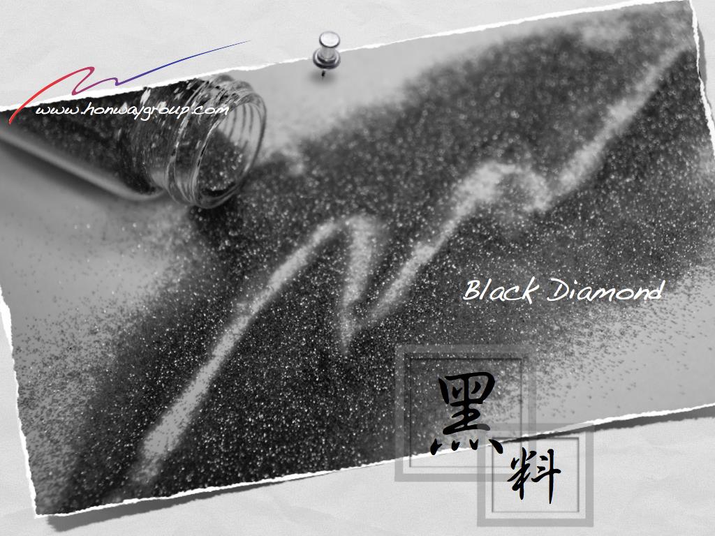
Our Honway polishing and conditioning solutions provide stable dressing assistance from the process’s beginning to its end. Both our diamond polishing liquid and diamond disks ensure workpieces achieve ultimate surface finishes.
| Category | Elemental Semiconductor | Compound Semiconductor | ||
| Representative Materials | Silicon (Si), Germanium (Ge) | Gallium Arsenide (GaAs), Indium Phosphide (InP) | Silicon Carbide (SiC) | Gallium Nitride (GaN) |
| Characteristics | Currently the main semiconductor material; low cost, mature technology, complete supply chain; suitable for everyday applications. | High frequency, high efficiency, low power consumption; but cannot withstand excessively high voltage. | High temperature and high pressure resistance, fast heat dissipation, fast switching speed, low loss, radiation resistant; suitable for 100KW-1MHz applications. | High frequency, high efficiency, high temperature and high pressure resistance. Suitable for applications below 1MW and above 100kHz. |
| Main Applications | Logic ICs, Analog ICs, Memory ICs, Micro-component ICs | Mobile phone power amplifiers, optical fiber transmission, lighting equipment, lasers | Electric vehicles, green energy generation equipment (solar, wind power), rail transport | 5G/6G high-frequency communication, satellite communication, LiDAR |
| Process Challenges | Requires precise processing of wafer surfaces and edges. | High requirements for wafer flatness and surface finish. | Material is extremely hard, high processing difficulty; requires ultra-precision grinding and polishing. (This is Honway’s professional field in diamond polishing slurry and grinding wheels. ) | Material is extremely hard, high processing difficulty; requires ultra-precision grinding and polishing. (This is Honway’s professional field in diamond polishing slurry and grinding wheels. ) |
Honway Solutions: Diamond Machining Tools Tailored for Different Semiconductor Materials
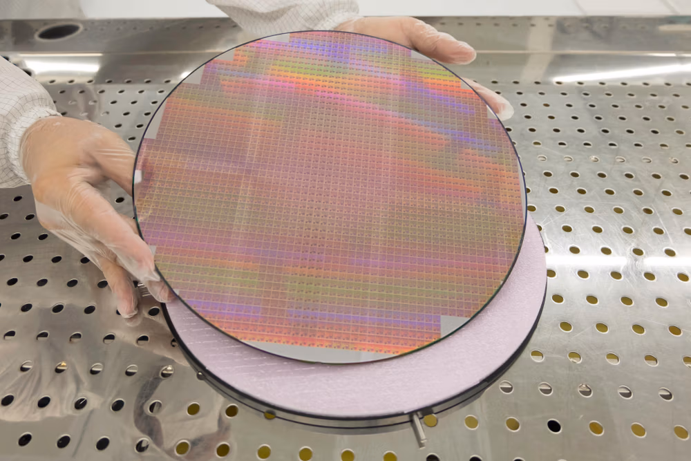
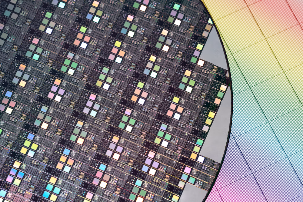
Honway deeply understands that whether it’s the widely adopted silicon wafers or emerging compound semiconductors like GaAs, InP, SiC, and GaN, each material faces unique challenges in precision manufacturing. It is precisely these challenges that drive our ultimate pursuit of diamond industrial consumable solutions.
1. First-Generation Semiconductors (Elemental Semiconductors): Silicon (Si), Germanium (Ge)
- Process Challenges: The key to silicon wafer processing lies in achieving extreme flatness and integrity of the wafer surface and edges. Any microscopic defect will impact the final component performance and yield.
- Honway’s Key Tools:
- Chamfering and Grinding Wheels for Silicon Wafers: Ensure smooth and damage-free edges for silicon wafers, effectively preventing chipping.
- Grinding Wheels for Wafer Surface Grinding: Achieve ultimate flatness for silicon wafer surfaces, serving as the foundation for efficient processes.
- Honway Diamond Polishing Liquid: Offers a variety of nano-particle size options, capable of achieving mirror-finish polishing (Ra ≤ 0.01 µm) results, significantly improving component performance and yield.
- Honway Polishing Pads: In conjunction with polishing liquid (slurry) and downforce, remove excess material from the wafer surface, such as oxide layers, dielectric layers (ILD), and metal layers (e.g., Cu, W), ensuring process stability.
- Honway Wafer Dicing Blade Series: Designed for various hard and brittle materials such as semiconductor wafers and packaging substrates, this series includes high-precision electroplated blades, stable and wear-resistant hard blades, and high-speed, long-life soft blades, comprehensively meeting the demands for high efficiency and high yield in wafer dicing and backend packaging.
※Diamond Disk Consultation:
Introduction: Through its high hardness, precisely conditions grinding pads and polishing pads, ensuring the flatness and cutting performance of the polishing pad, maintaining optimal cutting performance to sustain the flatness and rate during wafer polishing, and improving yield.
Services Provided: If you wish to learn more detailed information, please contact Honway. Honway provides professional related services to tailor a personalized project for you.
Second-Generation Compound Semiconductors: Gallium Arsenide (GaAs), Indium Phosphide (InP)
- Process Challenges: These high-frequency optoelectronic materials demand extremely high flatness and smoothness for wafers, directly impacting the high-frequency characteristics and optoelectronic performance of components.
- Honway’s Key Tools:
- Grinding Wheels for Wafer Surface Grinding: Precisely grinds these high-frequency optoelectronic material wafers, ensuring the wafer surface achieves nanometer-level ultra-high flatness.
- Honway Diamond Polishing Liquid: Provides a variety of nano-particle size options, capable of delivering ultimate surface finish (Ra ≤ 0.01 µm), ensuring excellent optoelectronic and electrical performance of components.
- Honway Polishing Pads: In conjunction with polishing liquid (slurry) and downforce, remove excess material from the wafer surface, such as oxide layers, dielectric layers (ILD), and metal layers (e.g., Cu, W), improving the production yield of critical components.
- Honway Wafer Dicing Blade Series: Designed for various hard and brittle materials such as semiconductor wafers and packaging substrates, this series includes high-precision electroplated blades, stable and wear-resistant hard blades, and high-speed, long-life soft blades, comprehensively meeting the demands for high efficiency and high yield in wafer dicing and backend packaging.
※Diamond Disk Consultation:
Introduction: Through its high hardness, precisely conditions grinding pads and polishing pads, ensuring the flatness and cutting performance of the polishing pad, maintaining optimal cutting performance to sustain the flatness and rate during wafer polishing, and improving yield.
Services Provided: If you wish to learn more detailed information, please contact Honway. Honway provides professional related services to tailor a personalized project for you.
3. Third-Generation Compound Semiconductors: Silicon Carbide (SiC), Gallium Nitride (GaN)
- Process Challenges: Due to the extreme hardness of these materials, processing difficulty is exceptionally high, leading to unprecedented demand for ultra-precision grinding and polishing.
- Honway’s Key Tools:
- Grinding Wheels for Wafer Surface Grinding: Specifically designed for these ultra-hard materials, capable of precise grinding and ensuring flatness, marking the first step in overcoming processing difficulties.
- Honway Diamond Polishing Liquid: Optimized for the characteristics of SiC and GaN, capable of achieving industry-leading surface smoothness, which is crucial for component performance.
- Honway Polishing Pads: In conjunction with Honway diamond polishing liquid and downforce, efficiently remove wafer surface materials such as oxide layers, dielectric layers (ILD), and metal layers (e.g., Cu, W), crucial for ensuring the process yield of SiC and GaN.
- Honway Wafer Dicing Blade Series: Designed for various hard and brittle materials such as semiconductor wafers and packaging substrates, this series includes high-precision electroplated blades, stable and wear-resistant hard blades, and high-speed, long-life soft blades, comprehensively meeting the demands for high efficiency and high yield in wafer dicing and backend packaging.
※Diamond Disk Consultation:
Introduction: Through its high hardness, precisely conditions grinding pads and polishing pads, ensuring the flatness and cutting performance of the polishing pad, maintaining optimal cutting performance to sustain the flatness and rate during wafer polishing, and improving yield.
Services Provided: If you wish to learn more detailed information, please contact Honway. Honway provides professional related services to tailor a personalized project for you.
Applications and Future Trends of Compound Semiconductors
With the rapid development of emerging fields such as 5G/6G communication, electric vehicles, and renewable energy, the application market for compound semiconductor materials continues to expand, with broad development prospects.

Main Application Areas:
- High-Power Electronics and Electric Vehicles: SiC and GaN, due to their advantages in high-temperature and high-voltage resistance, high conversion efficiency, and low loss, have become key materials for core electronic components in electric vehicle (EV) battery chargers, wireless charging, and converters.
- Gallium Oxide (Ga₂O₃), with its ultra-wide bandgap, is expected to further extend the range of electric vehicles.
- High-Frequency Communication: 5G/6G communication technology requires higher frequency and more efficient radio frequency components. GaAs and GaN have inherent advantages in high-frequency communication and are widely used in radio frequency (RF) and millimeter-wave communication systems
- Optoelectronic Components: GaN can be applied in LED lighting, such as UV-LEDs; GaN lasers are used in medical, automotive, and lighting. GaAs and InGaN can be used to improve solar panel efficiency.
- Renewable Energy: Solar inverters and wind turbines are important application fields for SiC in green energy generation equipment. Compound semiconductors have significant advantages in reducing energy loss and improving energy conversion efficiency.
- Medical and Sensors: GaN has potential in emerging product applications in the healthcare industry, such as wireless medical implants and wearable devices. GaAs and GaN are crucial for developing LiDAR (Light Detection and Ranging) sensors in autonomous vehicles, commonly used for distance measurement in automotive Advanced Driver-Assistance Systems (ADAS).
- Extreme Environment Applications: Wide bandgap materials, due to their excellent high-temperature and high-pressure resistance, have irreplaceable value in fields that demand extremely high component reliability and stability, such as military, defense, and aerospace.
Future Trend – Silicon Photonics (SiPh)
Compared to traditional electronic circuits, Silicon Photonics (SiPh) utilizes photons to transmit signals (with transmission rates exceeding 100 Gb/s), enabling high-speed, low-power Photonic Integrated Circuits (PICs). Chips manufactured with SiPh are not only small in size and low in energy consumption but can also be integrated with existing CMOS processes, aiding in large-scale production and application promotion.
This technology is mainly built on Silicon-on-Insulator (SOI) wafers, using standard semiconductor processes to fabricate components in the silicon layer. Silicon is transparent under infrared light, and when surrounded by silicon dioxide (SiO₂) or air, it can form effective light-guiding structures, allowing light to propagate with low loss within the chip.
Application Fields:
- Data Centers and High-Speed Data Communication
- Artificial Intelligence and High-Performance Computing (AI/HPC)
- Photonic Sensing and Biomedical Applications
- Quantum Computing and Quantum Communication (under exploration)
- Automotive and Laser Radar (LiDAR)
- 5G / 6G and Telecom Backbone Networks
Conclusion
In summary, semiconductors are the cornerstone driving global technological progress. From traditional silicon to cutting-edge compound semiconductors, material evolution continues towards high frequency, high performance, and extreme environment tolerance. Particularly, leading-edge applications such as 5G/6G communication, electric vehicles, and renewable energy are driving the immense market potential of wide bandgap materials like Silicon Carbide (SiC) and Gallium Nitride (GaN). Looking ahead, the rise of silicon photonics technology further heralds a new era for the semiconductor industry, moving towards higher integration and heterogeneous integration.
This semiconductor wave, driven by material and technological innovation, is not just a technological evolution but also an opportunity for market reshaping. Honway’s diamond industrial consumables are not just tools to help you improve yield and optimize efficiency; they are your solid backing for maintaining technological leadership and strengthening market competitiveness in this industry transformation. By partnering with Honway, you gain not only top-tier processing consumables but also the strategic advantage of ensuring long-term return on investment and leading future innovation.
We have helped companies double their grinding efficiency through our precision diamond consumable solutions, effectively reducing time costs.
Act now, and let’s together open a new chapter in semiconductor precision manufacturing!
- Free Consultation and Project Evaluation: Our Honway diamond industrial consumable experts provide product consultation and professional evaluation tailored to your specific process needs, working together to find the optimal grinding and polishing solution.
- Customized Solution Design: Whether you are facing challenges with silicon wafers or compound semiconductors (SiC, GaN, GaAs), we can customize the most suitable semiconductor grinding and polishing solutions for your needs.
- Advanced Materials and Performance Verification: We offer industry-leading Honway diamond polishing liquids, diamond disks, precision grinding wheels, and other consumables. We can also assist you with process implementation and performance verification to ensure your products achieve the expected high yield and excellent performance.
- Honway possesses stable supply capabilities, quality assurance, after-sales service, and customized support, ensuring the most consistent product quality for you.
Don’t let processing challenges limit your innovation! Contact us now, and let Honway’s diamond industrial consumables be your key to success!
More Information on Honway Diamond Grinding and Polishing Consumables:
To learn more about how Honway can bring breakthrough benefits to your semiconductor processes, please click the links below to explore our full range of diamond grinding and polishing consumables and technical details:
- Honway Nanodiamond Polishing Liquid Series
- Honway Precision Wafer Grinding and Polishing Pads
- Honway Grinding Wheels for Wafer Surface Grinding
- Honway Chamfering and Grinding Wheels for Silicon Wafers
- Honway Wafer Electroplated Dicing Blade
- Honway Wafer Packaging Dicing Blade – Soft Blade
- Honway Wafer Packaging Dicing Blade – Hard Blade
You can also directly “contact our Honway expert team,” and we will provide the most professional customized consultation and solutions.
Read More Related Topics
1. Diamond Substrate>>>From Jewelry to Semiconductors: Diamond as a Key Material for Next-Generation Thermal Management
We offer customized adjustments to the grinding process, tailored to meet processing requirements for maximum efficiency.
After reading the content, if you still don’t know how to select the most suitable option,
Feel free to contact us and we will have specialist available to answer your questions.
If you need customized quotations, you’re also welcome to contact us.
Customer Service Hours: Monday to Friday 09:00~18:00 (GMT+8)
Phone: +8867 223 1058
If you have a subject that you want to know or a phone call that is not clear, you are welcome to send a private message to Facebook~~
Honway Facebook: https://www.facebook.com/honwaygroup
You may be interested in…
[wpb-random-posts]