
As traditional silicon chip manufacturing processes approach their limits, scientists are actively seeking new materials to continue the trend of Moore’s Law.
Among these, Transition Metal Dichalcogenides (TMDs) have emerged as highly promising candidate materials.
A recent study by a research team at the U.S. Department of Energy’s (DOE) Princeton Plasma Physics Laboratory (PPPL) delves into the impact of TMDs’ atomic structure and internal defects on their electrical properties, laying the groundwork for the development of next-generation high-performance chips.
Table of Contents
From Silicon Chips to TMDs: The Evolution of Semiconductor Technology
Traditional silicon chips have underpinned computing technology for over half a century. However, the minimum feature size of current commercial chips has shrunk to 3 nanometers, nearing the physical limit. With the ever-increasing demand for higher-performance computing, scientists are turning to two-dimensional materials, hoping to break through the limitations of existing technology.
TMDs, as a type of two-dimensional material, are composed of only a few layers of atoms, with a thickness that can be as thin as three atoms. (You can imagine it as a tiny metal sandwich.)
TMDs exhibit different physical, chemical, and electronic properties compared to traditional silicon materials. Unlike graphene, the most well-known two-dimensional material, TMDs are composed of transition metals (such as Molybdenum Mo, Tungsten W, metals from Group 3 to Group 12 of the periodic table) and chalcogen elements (such as Sulfur S, Selenium Se, Tellurium Te). Their special layered structure gives them excellent electronic and optical properties, making them a hot research topic in the semiconductor field.
Research Findings: Internal Defects and Electrical Properties of TMDs
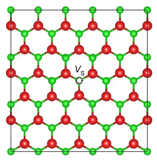
The crystal structure of TMDs is not perfect; defects within them can affect or even enhance their electronic performance. For example, an atom may be missing from the atomic lattice, or an extra atom may appear in an unexpected location. While these defects can affect the material’s conductivity, certain specific defects can actually improve the semiconductor properties of TMDs.
Research by the PPPL physicist Shoaib Khalid’s team found that bulk TMDs often contain extra electrons, and these electrons may be caused by hydrogen.
The research team calculated the formation energy of different defect types to determine which defects are most likely to occur and analyzed how these defects affect the material’s charge transport properties.
The results showed that hydrogen-related defects may cause TMDs to exhibit n-type (negatively charged) semiconductor properties, while chalcogen vacancies may alter the material’s optical and electronic properties.
Applications of TMDs in Future Chip Manufacturing
The researchers suggest that “photoluminescence” technology can be used to analyze defects inside TMDs by measuring the frequency of light emitted by the material to infer changes in the atomic structure.
This research provides experimental guidance for future TMD applications, especially in the development of next-generation computer chips, helping engineers design TMD semiconductors that meet application requirements.
With technological advancements, experts predict that TMD chips could be practically applied in electronic devices as early as 2030, becoming a strong alternative to silicon chips. By in-depth research on material structure and defect effects, scientists will be able to further optimize the performance of TMDs, driving semiconductor technology forward.
Reference
- Beyond Silicon: How Atom-Thin Materials Are Revolutionizing Chips
- Replacing Silicon with TMD Materials to Advance Smaller, More Efficient Semiconductor Chips for the Next Generation
- Shoaib Khalid、Anderson Janotti 和 Bharat Medasani (2024). Role of chalcogen vacancies and hydrogen in the optical and electrical properties of bulk transition-metal dichalcogenides, 2D Materials, Volume 11, Number 3, DOI 10.1088/2053-1583/ad4720.
( First image source: Princeton Plasma Physics Laboratory)
We offer customized adjustments to the grinding process, tailored to meet processing requirements for maximum efficiency.
Feel free to contact us and we will have specialist available to answer your questions.
If you need customized quotations, you’re also welcome to contact us.
Customer Service Hours: Monday to Friday 09:00~18:00 (GMT+8)
Phone: +8867 223 1058
If you have a subject that you want to know or a phone call that is not clear, you are welcome to send a private message to Facebook~~
Honway Facebook: https://www.facebook.com/honwaygroup
You may be interested in…
[wpb-random-posts]