In semiconductor manufacturing, wafer flatness is crucial for precise circuit stacking. Chemical Mechanical Planarization (CMP) technology plays the role of a “wafer skin resurfacer,” combining chemical and mechanical actions to precisely remove excess material from the wafer surface, laying a perfect foundation for subsequent processes.
Honway, deeply rooted in the field of semiconductor grinding and polishing, understands that ultimate wafer flatness is the cornerstone for achieving high-performance chips. Faced with increasingly stringent process challenges, we provide comprehensive and efficient CMP core consumable solutions, covering a wide range of high-performance polishing materials such as diamond, aluminum oxide, cerium oxide, and silicon dioxide. We can comprehensively assist in wafer processing from rough grinding to mirror-finish polishing, laying a perfect foundation for your precision processes.
Table of Contents
What is CMP?

CMP, short for Chemical Mechanical Planarization, also known as Chemical Mechanical Polishing, is an extremely critical process in semiconductor manufacturing.
Simply put, CMP is like a “skin resurfacing” technique for semiconductor wafers. It combines the forces of chemical corrosion and mechanical grinding, aiming to make the wafer surface both flat and smooth. This technology uses polishing slurries containing nano-sized abrasives and polishing pads, precisely controlled to remove excess material from the wafer, achieving flatness at the micrometer or even nanometer level, ultimately resulting in a “mirror-like” glossy effect on the wafer surface.
Why Do Semiconductors Need Grinding and Polishing?

In the semiconductor manufacturing process, to form complex circuits, multiple layers of materials need to be stacked on the wafer. Imagine building a skyscraper: each floor must be flat to ensure the stability of the next. Similarly, if a semiconductor wafer has uneven surfaces or defects in each process step, this will seriously affect the final chip’s yield and performance.
Reasons Why the CMP Process is Indispensable:
- Ensuring Precise Circuit Stacking: CMP’s primary function is planarization. It can reduce or eliminate height variations generated during repetitive process stacking, ensuring uniform thickness and flat surfaces for each circuit layer, providing an ideal foundation for subsequent photolithography and etching processes.
- Improving Chip Yield and Performance: By precisely controlling the material removal amount, CMP can prevent over-polishing or under-polishing, ensuring that the circuits in the chip can be formed accurately, thereby improving chip performance and manufacturing yield.
- Controlling Wafer Thickness: In addition to surface planarization, the grinding process is also used to thin wafers. For example, back grinding (BG) reduces wafer thickness from an initial 800-700 micrometers to 80-70 micrometers, and can even be thinned to about 20 micrometers through multi-layer stacking technologies. This is crucial for applications such as multi-chip packaging (MCP), as it allows for more layers of circuit stacking within a limited height, meeting the demands for miniaturization and high integration in electronic products.
- Removing Surface Defects and Residues: Grinding and polishing can also improve micro-defects left by previous processes and remove residual materials from the wafer surface, making the surface brighter and ready for the next process. This step is critical for ensuring chip quality and reliability.
Wafer Specification Requirements After Grinding and Polishing
In semiconductor manufacturing, wafers must meet extremely strict physical and surface specifications after back grinding and precision polishing to ensure the reliability of subsequent processes and chip performance. The main requirements can be divided into three aspects:
1. Thickness Control:
- Standard Variation:
- Initial wafer thickness: approximately 700–800 micrometers (µm).
- Thickness after general grinding: Reduced to 70–80 micrometers.
- Advanced MCP (Multi-Chip Package) requirements: Can be further thinned to approximately 20 micrometers.
- Challenges: Excessive thickness leads to poor heat dissipation; too thin makes it fragile, especially with the widespread use of 12-inch wafers, the difficulty of thickness control increases with packaging trends.
2. Surface Flatness and Roughness (Ra Value):
- Roughness Indicator:
- Measured using Ra value (Roughness Average).
- A smaller Ra value indicates a smoother surface, ideally approaching atomic-level flatness.
- Potential Risks:
- Surface unevenness will affect circuit pattern transfer, causing component performance deviation or failure.
- Internal stress can induce surface deformation, potentially leading to parameter drift or decreased reliability.
3. Defect Control:
- Control Range:
- Surface damage.
- Micro-crack generation.
- Particle and foreign object contamination.
- Importance: Even minor contamination can escalate into fatal defects in subsequent processes, leading to chip scrapping.
- Thin Wafer Risk: The thinner the wafer, the higher its mechanical fragility, and the lower its tolerance for particle impact or mechanical interference from carriers during processing, requiring particular caution.
Challenges Encountered When Grinding Semiconductor Materials
- Precision of Material Removal and Surface Uniformity: The fine structures of semiconductor components require grinding processes to precisely control the amount of material removed and maintain a high degree of flatness and uniformity. This necessitates precise selection of abrasive types (such as aluminum oxide, silicon dioxide, or diamond) and particle size distribution to ensure optimal results.
- Surface Uniformity: The ground surface must possess a high degree of flatness and uniformity. Any localized uneven grinding will lead to failures in subsequent photolithography and etching processes, thereby affecting overall chip performance.
- Defect Control: The grinding process is prone to introducing defects such as surface damage, micro-cracks, and particle contamination. Even tiny defects can lead to component failure, so they must be effectively controlled and minimized. Especially as wafers become thinner, the probability of defect generation increases, and the difficulty of subsequent processes also increases.
- Stress Generation and Impact: During the grinding process, the contact between the grinding head and the wafer surface generates shear stress and pressure, and the flow of chemical solutions and abrasives also applies stress. These stresses may cause plastic deformation and residual stress on the wafer surface, affecting the final flatness and roughness, and even influencing electrical performance, leading to component parameter drift and decreased product yield.
- Processing Difficulty of Superhard Special Materials: For third-generation semiconductor materials such as silicon carbide (SiC) and gallium nitride (GaN), their extreme hardness presents unprecedented challenges to traditional grinding. These materials particularly require superhard abrasives like diamond to achieve efficient and low-damage removal.
How to Improve Wafer Flatness
To overcome the above challenges and improve wafer flatness, the industry adopts various strategies:
- Optimize Processing Parameters:
- Grinding Fluid and Abrasive Selection: Precisely control the flow rate and concentration of the grinding fluid, and accurately select the most suitable abrasive type (such as aluminum oxide, cerium oxide, silicon dioxide, or diamond) and its particle size distribution (e.g., 50-250 nanometers, effectively controlling agglomerates of 1-10 micrometers) based on different semiconductor materials and grinding targets. The chemical properties of the grinding fluid and abrasive characteristics must perfectly match to achieve uniform and efficient material removal and surface effects.
- Grinding Force Control: Precisely control parameters such as grinding pressure, speed, and time to achieve optimal grinding results, avoiding excessive pressure that leads to damage or insufficient pressure that affects efficiency.
※Industry Principle for Grinding – CMP Rework Principle [Thick over Thin]: When adjusting parameters, it is recommended that the actual time in seconds be shorter than the estimated time. It is better to leave thickness than to go too thin, as this allows for the possibility of rework.
- Multi-Step Grinding Process: Adopt multi-step grinding and polishing processes, such as rough grinding, fine grinding, and even using the scribe-and-grind method (DBG) when wafer thickness is less than 50 micrometers. This involves scribing before the first grinding, then grinding and a second scribing to safely separate the chips and reduce external defects during grinding. This gradual refinement method can effectively reduce stress and obtain a smoother surface.
- Local Heating and Chemical Etching: Introducing local heating during the grinding and polishing process can change the physical properties of the wafer, thereby reducing the impact of stress. In addition, with technological development, introducing chemical etching technology from semiconductor front-end processes, combined with mechanical grinding, to comprehensively develop new processing methods is also a direction for solving grinding bottlenecks.
- Grinding Pad Selection and Maintenance: The material and characteristics of the grinding pad directly affect the grinding effect and stability. Regularly monitoring its wear and contamination and performing maintenance are important steps to ensure process quality.
- Supply Chain and Procurement Strategy: Select high-quality grinding material and equipment suppliers, and optimize procurement processes to ensure compliance with production needs and process requirements.
- Continuous Improvement and Standardization: Establish Standard Operating Procedures (SOPs) to reduce variability, and regularly train production teams on stress management and process optimization. Simultaneously, continuously evaluate and optimize the grinding and polishing process based on actual production data to meet the challenges posed by the continuous development of semiconductor technology.
Key Grinding Tools for CMP
Chemical Mechanical Planarization (CMP) is crucial for ensuring ultimate wafer flatness. Honway, with its rich experience in precision grinding and polishing, provides a full range of high-performance CMP core consumables that can meet the diverse needs from traditional silicon wafers to emerging compound semiconductors. Our solutions cover precision grinding wheels, various polishing liquids (such as diamond, aluminum oxide, cerium oxide, silicon dioxide), polishing pads, and diamond disks, aiming to provide semiconductor manufacturers with comprehensive and optimized solutions to help improve wafer quality and overcome process limitations.
Product List:
- Honway Precision Grinding Wheel Series:
- Chamfering and Grinding Wheels for Silicon Wafers: Ensure smooth and damage-free edges for silicon wafers, effectively preventing chipping.
- Grinding Wheels for Wafer Surface Grinding: Achieve ultimate flatness for silicon wafer surfaces, serving as the foundation for efficient processes.
- Compound semiconductor special grinding wheel: Provides efficient and low-damage rough grinding solutions for super-hard materials such as SiC/GaN.
- Honway High-Performance Polishing Liquid Series:
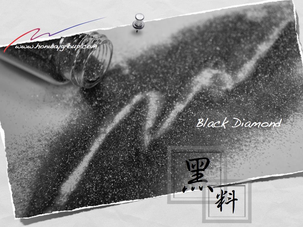
- Honway Diamond Polishing Liquid: Provides a variety of nano-particle size options, especially suitable for mirror-finish polishing (Ra ≤ 0.01 µm) of ultra-hard materials such as SiC and GaN, significantly improving component performance and yield.
- Honway Aluminum Oxide Polishing Liquid: Suitable for various metal layers, such as copper, tungsten, and dielectric layers in CMP, providing excellent material removal rate and surface quality.
- Honway Cerium Oxide Polishing Liquid: Primarily used for shallow trench isolation (STI) and dielectric layer planarization, providing high selectivity and low-defect polishing results.
- Honway Silicon Dioxide Polishing Liquid: Widely used for fine polishing of dielectric layers and silicon wafers, providing excellent surface flatness and low defect rate.
- Honway Precision Wafer Grinding and Polishing Pads: In conjunction with different types of polishing liquids (slurry) and downforce, remove excess material from the wafer surface, such as oxide layers, dielectric layers (ILD), and metal layers (e.g., Cu, W), ensuring process stability.
- Honway Wafer Dicing Blade Series:
- Wafer Electroplated Dicing Blade: Features an ultra-small kerf and high precision, suitable for silicon wafers and various compound semiconductor materials.
- Wafer Packaging Dicing Blade – Hard Blade: Stable blade with excellent wear resistance, effectively controls die size, suitable for dicing LED and packaging substrates.
- Wafer Packaging Dicing Blade – Soft Blade: Offers high cutting speed and a long lifespan, ideal for mass production applications on substrates like PCBs, EMC, and various hard and brittle materials.
- Honway Diamond Disk Consultation:
- Introduction: As a “conditioner” for grinding/polishing pads, the diamond disk, through its high hardness, precisely conditions the grinding/polishing pad surface, ensuring its flatness and cutting performance, maintaining optimal cutting performance to sustain the flatness and rate during wafer polishing, and improving yield.
- Services Provided: If you wish to learn more detailed information, please contact Honway. Honway provides professional related services to tailor a personalized project for you.
Act now, and let’s together open a new chapter in semiconductor precision manufacturing!
- Free Consultation and Project Evaluation: Our Honway diamond industrial consumable experts provide product consultation and professional evaluation tailored to your specific process needs, working together to find the optimal grinding and polishing solution.
- Customized Solution Design: Whether you are facing challenges with silicon wafers or compound semiconductors (SiC, GaN, GaAs), we can customize the most suitable semiconductor grinding and polishing solutions for your needs.
- Advanced Materials and Performance Verification: We offer industry-leading Honway diamond polishing liquids, diamond disks, precision grinding wheels, and other consumables. We can also assist you with process implementation and performance verification to ensure your products achieve the expected high yield and excellent performance.
- Honway possesses stable supply capabilities, quality assurance, after-sales service, and customized support, ensuring the most consistent product quality for you.
Don’t let processing challenges limit your innovation! Contact us now, and let Honway’s diamond industrial consumables be your key to success!
More Information on Honway Diamond Grinding and Polishing Consumables:
To learn more about how Honway can bring breakthrough benefits to your semiconductor processes, please click the links below to explore our full range of diamond grinding and polishing consumables and technical details:
- Honway Nanodiamond Polishing Liquid Series
- Honway Precision Wafer Grinding and Polishing Pads
- Honway Grinding Wheels for Wafer Surface Grinding
- Honway Chamfering and Grinding Wheels for Silicon Wafers
- Honway Wafer Electroplated Dicing Blade
- Honway Wafer Packaging Dicing Blade – Soft Blade
- Honway Wafer Packaging Dicing Blade – Hard Blade
You can also directly “contact our Honway expert team,” and we will provide the most professional customized consultation and solutions.
Read More Related Topics
- Diamond Substrate>>>From jewelry to semiconductors: Diamonds play a key role in the next generation of thermal conductivity materials
- Compound Semiconductors>>>The secret weapon of semiconductor precision manufacturing: diamond grinding and polishing consumables, effectively improving wafer yield and performance!
We offer customized adjustments to the grinding process, tailored to meet processing requirements for maximum efficiency.
After reading the content, if you still don’t know how to select the most suitable option,
Feel free to contact us and we will have specialist available to answer your questions.
If you need customized quotations, you’re also welcome to contact us.
Customer Service Hours: Monday to Friday 09:00~18:00 (GMT+8)
Phone: +8867 223 1058
If you have a subject that you want to know or a phone call that is not clear, you are welcome to send a private message to Facebook~~
Honway Facebook: https://www.facebook.com/honwaygroup
You may be interested in…
[wpb-random-posts]