In the semiconductor and optoelectronics industries, there is an element that, while not as widely known as silicon, holds a pivotal position in both history and modern applications—that is Germanium (Ge). Since its discovery in 1886, Germanium has gradually become a core material for key technologies such as electronics, fiber optics, infrared optics, and solar cells, owing to its unique semiconductor properties, excellent infrared transparency, and controllable high purity. This article will take you through the historical origins, physical and chemical properties, purity specifications, and broad applications of Germanium in the semiconductor and other industries.
Table of Contents
Historical Origin and Discovery
In 1869, when the Russian chemist Dmitri Mendeleev proposed the periodic law of chemical elements, he predicted the existence of an unknown element that should lie between silicon and tin, temporarily naming it “Ekasilicon.” It wasn’t until 1886 that the German chemist Clemens Winkler formally discovered the new element while analyzing a rare silver-germanium sulfide mineral called Argyrodite, naming it “Germanium” after his homeland, Germania.
Subsequently, Winkler prepared various germanium compounds and further verified their physical and chemical properties, confirming Mendeleev’s prediction and marking an important milestone for the periodic table.
Introduction to Germanium
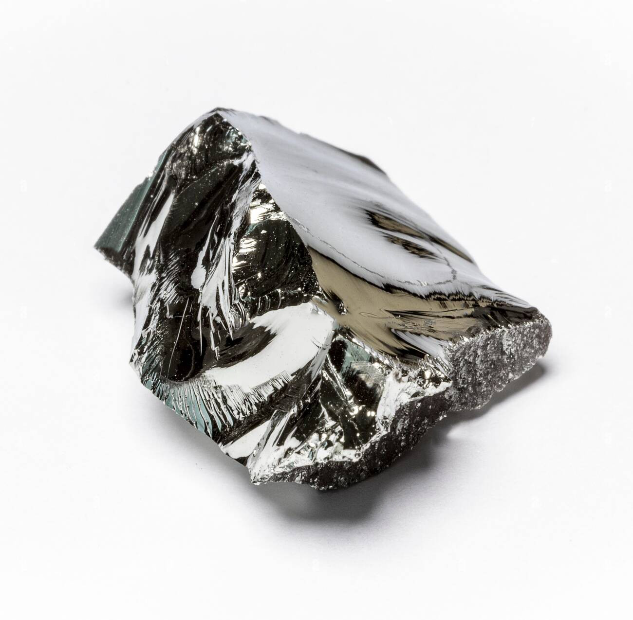
Germanium, with the chemical symbol Ge and atomic number 32, is a gray-white metalloid with a metallic luster. It belongs to the carbon group elements and shares similar chemical properties with silicon and tin, possessing excellent electrical and optical performance.
Germanium is an important semiconductor material with a crucial role in modern industry, applied in fiber optic communication, infrared optics, solar cells, nuclear detection, and electronic components.
Physical Properties
- Atomic Weight: 72.61
- Density: 5.35 g/cm³
- Melting Point: 938.25°C
- Boiling Point: 2830°C
- Appearance: Grayish-white solid, hard but brittle
- Refractive Index: 4.0034 (Suitable for infrared optics)
- Thermal Conductivity: 59.8 W/m·K
- Specific Heat Capacity: 319 J/kg·K
- Young’s Modulus: 102.7 GPa
- Knoop Hardness: 780
Germanium exhibits volume expansion upon solidification, a property shared by only a few substances, such as water and silicon.
Chemical Properties
- It slowly oxidizes at 250°C to form germanium dioxide (GeO2).
- Insoluble in dilute acids and alkalis but soluble in concentrated sulfuric acid.
- Reacts with molten strong alkalis to form germanates (GeO32−).
- Common compounds include Germanium Tetrachloride (GeCl4) and Germane (GeH4).
Other qualities
- Isotopes: Five stable isotopes exist in nature (Ge-70 to Ge-76).
- Optical Performance: High transparency in the 1.8 – 12 µm infrared band, suitable for manufacturing infrared lenses.
- Mechanical Performance: High hardness with good processing stability.
Purity and Specifications
The application of Germanium depends on its purity, with different industries imposing strict requirements on impurity content:
| Specification | Purity | Detection of impurities | Total impurity content | Scope of Application | |
| High purity germanium (5N) | 99.999% | Al、Ca、Co、Fe、Mg、Ni、Cu、In、Zn、Si、Pb、As | <10ppm | For general electronics and optics | |
| Ultrapure Germanium (6N) | 99.9999% | Al、Ca、Co、Fe、Mg、Ni、Cu、In、Zn、Si、Pb、As | <1ppm | For high-precision electronics and optical fibers | |
| Ultra-high germanium oxide (7N) | 99.9999% | Al、Ca、Co、Fe、Mg、Ni、Cu、In、Zn、Si、Pb、As | <0.1ppm (other: Cl<200ppm) | Special applications (Cl<200 ppm) |
Scope of Application
- Semiconductor Components: Historically used in transistors, diodes, and rectifiers. Today, it remains an important material for infrared detectors and specialized circuits.
- Fiber Optic Communication: Germanium-doped optical fiber cores have a high refractive index, enhancing light transmission efficiency, making it a critical material for modern communication.
- Infrared Optics: Due to Germanium’s high transparency in the infrared range, it is widely used in infrared cameras, thermal imaging systems, and military night vision devices.
- Solar Cells: Used as the substrate material for III-V compound semiconductor (e.g., GaAs, InGaP) multi-junction solar cells, applied in the aerospace sector.
- Chemical Catalysts: Germanium compounds are used in polymerization reactions, driving plastic and chemical processes.
- Biomedicine: Some organogermanium compounds are being researched in the medical field.
Germanium’s Application in Semiconductors
Germanium is one of the earliest materials applied in the semiconductor industry:
World War II Era: The Birth of the Germanium Diode
In the 1940s, scientists discovered that Germanium possessed excellent unidirectional conductive properties. In 1941, the Germanium diode was first applied in WWII radar systems, successfully replacing vacuum tubes. This significantly boosted radar reception efficiency and established Germanium’s foundational status as a semiconductor material.
1948: The First Transistor
In the 1940s, scientists discovered that Germanium possessed excellent unidirectional conductive properties. In 1941, the Germanium diode was first applied in WWII radar systems, successfully replacing vacuum tubes. This significantly boosted radar reception efficiency and established Germanium’s foundational status as a semiconductor material.
1950–1970s: The Protagonist of the Electronics Industry
During this period, Germanium was widely used in transistors, diodes, and rectifiers, becoming the mainstream material in the electronics industry. Global annual Germanium production quickly grew from a few hundred kilograms to tens of metric tons, with demand sharply escalating.
After the 1970s: Replacement by Silicon
As silicon material purification technology matured, silicon gradually replaced Germanium as the core material of the semiconductor industry due to its lower cost and better thermal stability. Germanium’s market demand subsequently declined, and its applications gradually shifted toward specialized areas.
Modern Era: A Resurgence in High-End Applications
Despite being largely replaced by silicon, Germanium maintains its place in modern semiconductors thanks to its unique advantages:
- Silicon Germanium Alloy (SiGe): Widely used in radio frequency components, high-speed integrated circuits, and low-power devices.
- Fiber Optic Communication: Used as a dopant to increase the refractive index of the fiber core, enhancing light signal transmission efficiency.
- Multi-Junction Solar Cells: Germanium substrates support III-V semiconductor thin films, widely applied in aerospace solar cells.
With the increasing demand for high-speed computing, optoelectronic integration, and communication technology, Germanium is once again demonstrating its irreplaceable value.
More Honway raw material information
To learn more about how raw metals are driving next-generation technology, click on the links below to explore their properties, applications, and market prospects:
- Raw material – Arsenic (AS)
- Raw material – Selenium (Se)
- Raw material – tellurium (Te)
- Raw material-Indium (In)
- Raw materials – Antimony (Sb)
- Raw materials – Cadmium (Cd)
- Raw material-Gallium (Ga)
Read more about related topics:
- Gallium (Ga)>>>Gallium (Ga) – From Rare Metal to a Key Raw Material for Semiconductors and New Energy
- Cadmium (Cd) >>>Cadmium (Cd) – From Byproduct Metal to a Key Raw Material for Industry and Technology
You can also directly “contact our Honway expert team,” and we will provide the most professional customized consultation and solutions.
We offer customized adjustments to the grinding process, tailored to meet processing requirements for maximum efficiency.
After reading the content, if you still don’t know how to select the most suitable option,
Feel free to contact us and we will have specialist available to answer your questions.
If you need customized quotations, you’re also welcome to contact us.
Customer Service Hours: Monday to Friday 09:00~18:00 (GMT+8)
Phone: +8867 223 1058
If you have a subject that you want to know or a phone call that is not clear, you are welcome to send a private message to Facebook~~
Honway Facebook: https://www.facebook.com/honwaygroup
You may be interested in…
[wpb-random-posts]