Silicon Carbide (SiC) and Gallium Nitride (GaN), as new-generation Wide Bandgap Semiconductors (WBGS), are disrupting the application landscape of traditional silicon materials. They offer advantages such as high temperature and voltage resistance, high frequency, and low loss, making them particularly suitable for high-performance fields like electric vehicles, 5G/6G communication, renewable energy, and fast charging. Compared to silicon, SiC and GaN can maintain stable operation in more extreme environments while significantly reducing energy loss, pushing the global semiconductor industry into a new phase.
Table of Contents
SiC and GaN Advantages
Although both SiC and GaN are compound semiconductors, they each exhibit irreplaceable material advantages in the field of high-performance electronics.
Silicon Carbide (SiC)
- High breakdown voltage: Can withstand voltages far higher than silicon, making it suitable for high-voltage power applications.
- High thermal conductivity: Excellent heat dissipation efficiency, allowing for stable operation in high-temperature environments.
- Low on-resistance: Reduces energy loss and improves system efficiency.
Gallium Nitride (GaN)
- High electron mobility: Fast switching speed, suitable for high-frequency applications.
- High-frequency characteristics: Supports GHz-level operation, reducing component size and improving conversion efficiency.
- Low heat dissipation requirements: Reduces the size and cost of the heat dissipation system.
Both materials not only break through the limitations of traditional silicon-based materials in power and frequency but also lay a core foundation for high-performance, low-energy advanced electronic systems.
Key GaN Manufacturing Processes: HVPE and Ammonothermal Method
The substrate growth technology for GaN determines its performance and cost:
Hydride Vapor Phase Epitaxy (HVPE)
- Uses hydrogen gas as a carrier gas to react hydrogen chloride (HCl) with gallium (Ga) to produce gallium chloride (GaCl), which then reacts with ammonia (NH₃) to form GaN crystals.
- Process temperature is about 1000°C, allowing for rapid growth of a large amount of GaN.
- Disadvantage: Prone to cracks and lattice defects, resulting in poorer crystal quality.
Ammonothermal Method
- Uses supercritical ammonia as a solvent, which has both the dissolving ability of a liquid and the diffusion ability of a gas under high pressure and high temperature.
- Ga is dissolved by ammonia and then deposited to form GaN crystals.
- Advantages: Lower temperature, low energy consumption, low defect density, suitable for high-quality applications.
- Disadvantage: Slow growth rate, more complex process.
Key SiC Manufacturing Processes: Sublimation and Epitaxy
The manufacturing process for SiC is both time-consuming and difficult. From substrate growth to power component fabrication, every step is full of challenges.
Substrate Fabrication: Physical Vapor Transport (PVT) – Sublimation Method
This is the mainstream technology for producing SiC substrates. Its key process and challenges are as follows:
- Process Principle: SiC powder sublimates in a sealed environment at high temperature (approx. 2,200℃) and low pressure. The vapor then condenses and adheres to an SiC seed crystal to grow a SiC crystal.
- High Difficulty and Long Duration: Compared to silicon (Si) ingots, which can be grown to several meters in just a few days, an SiC ingot takes 2-3 weeks to grow to less than 10 cm, and the crystal growth quality cannot be monitored in real-time during the process, only confirmed at the very end.
- Subsequent Processing: After crystal growth is completed, it must go through multiple processes including cutting, grinding, and polishing to produce a smooth, specification-compliant substrate.
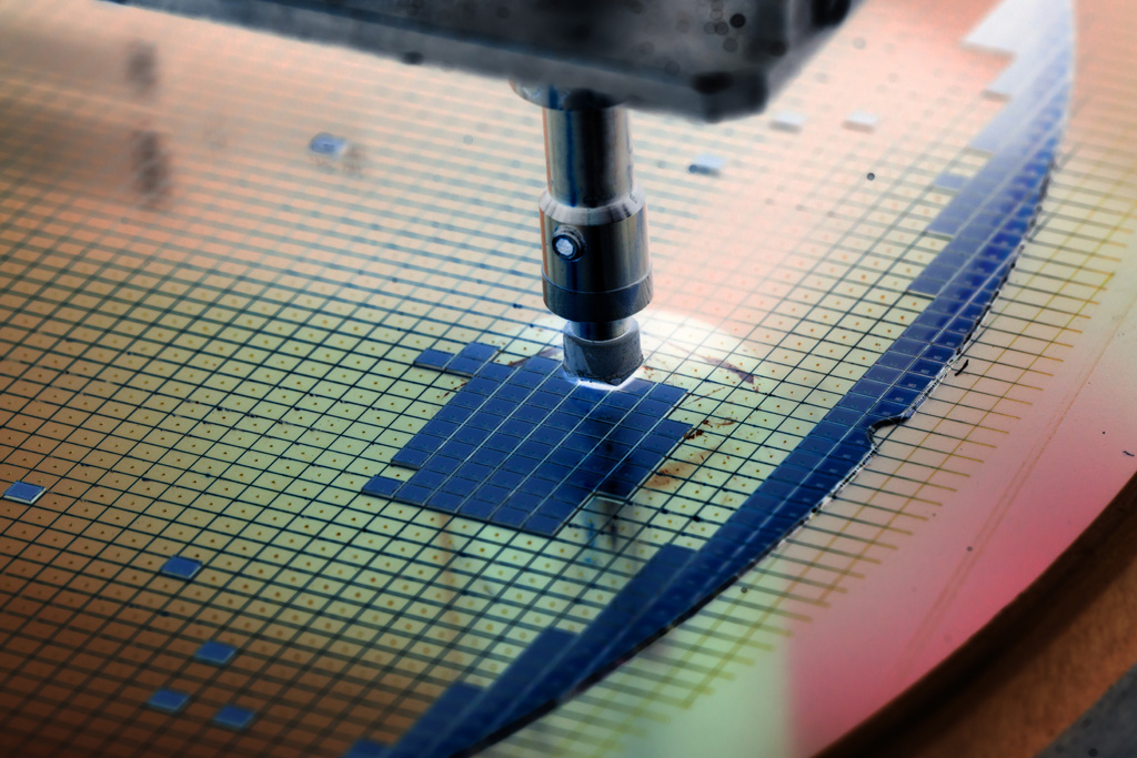
Epitaxy Phase: New Crystal on the Substrate

After the substrate is fabricated, an epitaxy step must be performed to grow a new crystal layer on the SiC substrate to form the structure of the power component.
- Technology Synchronization: Taiwan is synchronized with international standards in the basic epitaxy process technology.
- Component Design and New Processes: However, the design and process technology of SiC power components are interconnected. If there is a new component design, a new process technology often needs to be developed to match it, and Taiwan still needs more time to accumulate experience in this area.
The “Hardcore” Challenges of Grinding and Polishing SiC and GaN
In the manufacturing of high-performance power and high-frequency components, although SiC and GaN have excellent material properties, their ultra-high hardness, brittleness, and chemical inertness make grinding and polishing a technical bottleneck for the entire process. To more clearly present the challenges each material faces in the backend processes, the following lists four major challenges that may be encountered during the grinding and polishing of SiC and GaN, respectively:
SiC Grinding and Polishing Challenges
- Extreme Hardness and Brittleness: SiC has a Mohs hardness of 9.2, close to the diamond level. This, coupled with its high brittleness, results in low grinding efficiency and the potential for micro-cracks or wafer chipping with a slight mistake during processing, which reduces the wafer’s integrity rate.
- Chemical Inertness: The chemical stability of the SiC surface is extremely strong, making it difficult for traditional CMP slurries to act on it. This requires the introduction of highly active oxidizing agents or metal catalytic particles to form a removable oxide layer.
- Crystal Structure and Defects: Polytopes like 6H-SiC and 4H-SiC are anisotropic, leading to large differences in grinding rates. Defects such as micropipes and stacking faults can easily be magnified during processing, which reduces the yield of subsequent processes.
- Surface Integrity Requirements: Power components are extremely sensitive to surface flatness and defect density. Atomic-level roughness deviations can affect breakdown voltage, leakage current, and reliability.
GaN Grinding and Polishing Challenges
- High Hardness and Brittleness: GaN has a Mohs hardness of about 9. Its low cutting efficiency and high brittleness make thin wafers prone to cracking or chipping, and the risk is even higher in large-diameter wafer processing.
- Chemical Stability: GaN is chemically inert to both acidic and alkaline solutions, so CMP’s removal efficiency is low if it relies solely on chemical action. It needs to be combined with specific redox reactions or UV light to promote surface reactions.
- Crystal Structure and Heteroepitaxy Issues: Most GaN is grown heteroepitaxially, resulting in high interface stress and defect density. This leads to non-uniform removal rates during grinding, which can easily form steps or localized depressions.
- Surface and Interface Quality Requirements: High-frequency, high-power RF components have extremely high demands for surface and interface roughness. Atomic-level scratches or residual particles can affect component stability and power performance.
Overcoming the “Hard” Challenges of SiC and GaN: Honway’s Precision Grinding and Polishing Solutions
As compound semiconductor materials like SiC and GaN are becoming mainstream, especially with the trend towards 8-inch wafers, their extreme hardness and brittleness pose huge challenges to traditional grinding and polishing technology. These materials, with a Mohs hardness of 9.2-9.6, are prone to surface and sub-surface damage, warpage, and can affect subsequent component performance.
Honway Industrial addresses the physical properties of SiC and GaN by providing a comprehensive grinding and polishing solution from three aspects—consumables, process control, and equipment design—to help the industry break through bottlenecks and achieve stable process quality and high yield.
Grinding Phase: Stable Control from Rough to Fine Grinding
Traditional grinding tools often face problems such as long processing times, excessive sub-surface damage (SSD), and non-uniform thickness when processing SiC and GaN. Honway effectively solves these challenges through the following high-end consumables:
- Wafer-Specific Grinding Wheels: Adopt high-hardness, high-wear-resistance formulations that can rapidly remove material while effectively suppressing micro-crack generation, minimizing surface and sub-surface damage.
- Honway Grinding Pads: Stabilize pressure distribution and carrier flatness, ensuring the wafer does not warp during grinding, and precisely control thickness variation (TTV) and warpage (WARP), laying a good foundation for subsequent processes.
- Nano-grade Diamond Polishing Liquid: Designed for high-hardness materials, it incorporates surface structure modification and spherical diamond particles to significantly reduce grinding scratches and residual stress, reducing the burden on subsequent CMP processes.
- CMP Dressers: In the CMP process, dressers use diamonds or other high-hardness particles to precisely condition the polishing pad, removing residues and chemical deposits, restoring surface roughness, and preventing glazing that affects removal efficiency during long-term use.
CMP Polishing: Achieving Ultra-Flat, Damage-Free Surfaces
The performance of SiC and GaN components highly depends on the wafer’s surface flatness and defect control. This makes CMP (Chemical Mechanical Polishing) a core process for the entire manufacturing flow. Honway’s CMP solution is specifically designed for mirror-finish polishing of compound semiconductors:
- Five-Layer Structure CMP Polishing Pad: The innovative five-layer structure design has excellent rigidity and pressure adjustment capabilities, effectively controlling the material removal rate and ensuring surface uniformity. Its micro-pore and groove pattern design can improve slurry flow and reduce the risk of scratching.
- CMP Dresser: Uses diamonds or other high-hardness particles to precisely condition the polishing pad, removing residues generated during the process and preventing the “glazing” phenomenon. This ensures the polishing pad can continuously maintain stable cutting force and removal efficiency.
Polishing Liquid: The Core Key to Precise Chemical Etching and Selectivity
In the CMP process for SiC and GaN, chemical etching and the ability to selectively remove materials are crucial for determining the final surface quality. Honway provides exclusive formulations for various materials to ensure high performance and low defect rates:
- Dedicated Diamond Polishing Liquid: Designed for polishing compound semiconductors, it incorporates surface microstructure optimization and spherical diamond particles to effectively reduce processing scratches and SSD, achieving damage-free polishing and thereby improving the heat dissipation and reliability of power components. (In addition to spherical diamonds, other process diamond liquid options are also available to effectively solve various polishing problems).
In summary, Honway Precision, by integrating key consumables such as diamond polishing liquid, dedicated grinding wheels, and CMP polishing pads, provides high-performance, low-defect rate process solutions designed for SiC and GaN. This accelerates the mass production and application of these advanced materials in fields like power components, RF communication, and advanced packaging.
The Broad Prospects of SiC and GaN and the Continuous Innovation of Polishing Technology

With the growing demand for high-power, high-frequency components, the application prospects for SiC and GaN are becoming increasingly broad. SiC, with its high efficiency and low energy consumption, is becoming a core component in electric vehicle charging infrastructure and vehicle power systems. GaN, with its high-frequency characteristics and low power loss, is widely used in next-generation 5G RF modules and RF power amplifiers. In addition, both materials demonstrate excellent high-temperature resistance, radiation resistance, and high-power handling capabilities in cutting-edge fields like aerospace, satellite communication, and high-energy radar.
In response to the rapid expansion of application demands, grinding and polishing technology must also continue to break through. Future challenges include uniform processing of large-size SiC wafers, precise defect control of GaN heteroepitaxial wafers, and the realization of nano-level low-damage polishing. At the same time, combining intelligent processes with automated control will be key to improving efficiency, stability, and yield. Honway will continue to invest in R&D, integrating exclusive consumables with intelligent processes to drive innovation in SiC and GaN polishing technology and facilitate the mass production of high-performance semiconductor components.
More Information on Honway Diamond Grinding and Polishing Consumables:
To learn more about how Honway can bring breakthrough benefits to your semiconductor processes, please click the links below to explore our full range of diamond grinding and polishing consumables and technical details:
- Honway Nanodiamond Polishing Liquid Series
- Honway Precision Wafer Grinding and Polishing Pads
- Honway Grinding Wheels for Wafer Surface Grinding
- Honway Chamfering and Grinding Wheels for Silicon Wafers
- Honway Wafer Electroplated Dicing Blade
- Honway Wafer Packaging Dicing Blade – Soft Blade
- Honway Wafer Packaging Dicing Blade – Hard Blade
You can also directly “contact our Honway expert team,” and we will provide the most professional customized consultation and solutions.
Read More Related Topics
- Diamond Substrate>>>From jewelry to semiconductors: Diamonds play a key role in the next generation of thermal conductivity materials
- Compound Semiconductors>>>The secret weapon of semiconductor precision manufacturing: diamond grinding and polishing consumables, effectively improving wafer yield and performance!
- Semiconductor grinding and polishing>>>Grinding and Polishing in Semiconductor Manufacturing: Excellence from Material Selection to Consumable Empowerment
- Grinding and polishing cunsumbles>>>Innovative Grinding and Polishing Consumables: Driving the Semiconductor Industry Towards Higher Precision
- The key to ultra-flat wafers>>>The “Thin” Science of Semiconductor Grinding and Polishing: Key to Achieving Ultra-Flat Wafers
- Heterogeneous Integration and Advanced Packaging>>>Facing the Future: How Grinding and Polishing Consumables Empower Heterogeneous Integration and Advanced Packaging
- Polerowanie półprzewodników złożonych>>>Mastering Compound Semiconductor Polishing Technology: Achieving High Performance for Next-Generation Electronic Components
We offer customized adjustments to the grinding process, tailored to meet processing requirements for maximum efficiency.
After reading the content, if you still don’t know how to select the most suitable option,
Feel free to contact us and we will have specialist available to answer your questions.
If you need customized quotations, you’re also welcome to contact us.
Customer Service Hours: Monday to Friday 09:00~18:00 (GMT+8)
Phone: +8867 223 1058
If you have a subject that you want to know or a phone call that is not clear, you are welcome to send a private message to Facebook~~
Honway Facebook: https://www.facebook.com/honwaygroup
You may be interested in…
[wpb-random-posts]