With the rapid development of new-generation applications like artificial intelligence, high-performance computing, electric vehicles, and wireless communication, chip performance continues to climb. However, the accompanying high heat generation has become the biggest design challenge. As chips continue to miniaturize and power density constantly increases, thermal management issues are becoming more severe. Traditional heat dissipation materials like silicon and copper can no longer meet the demands of extreme applications.
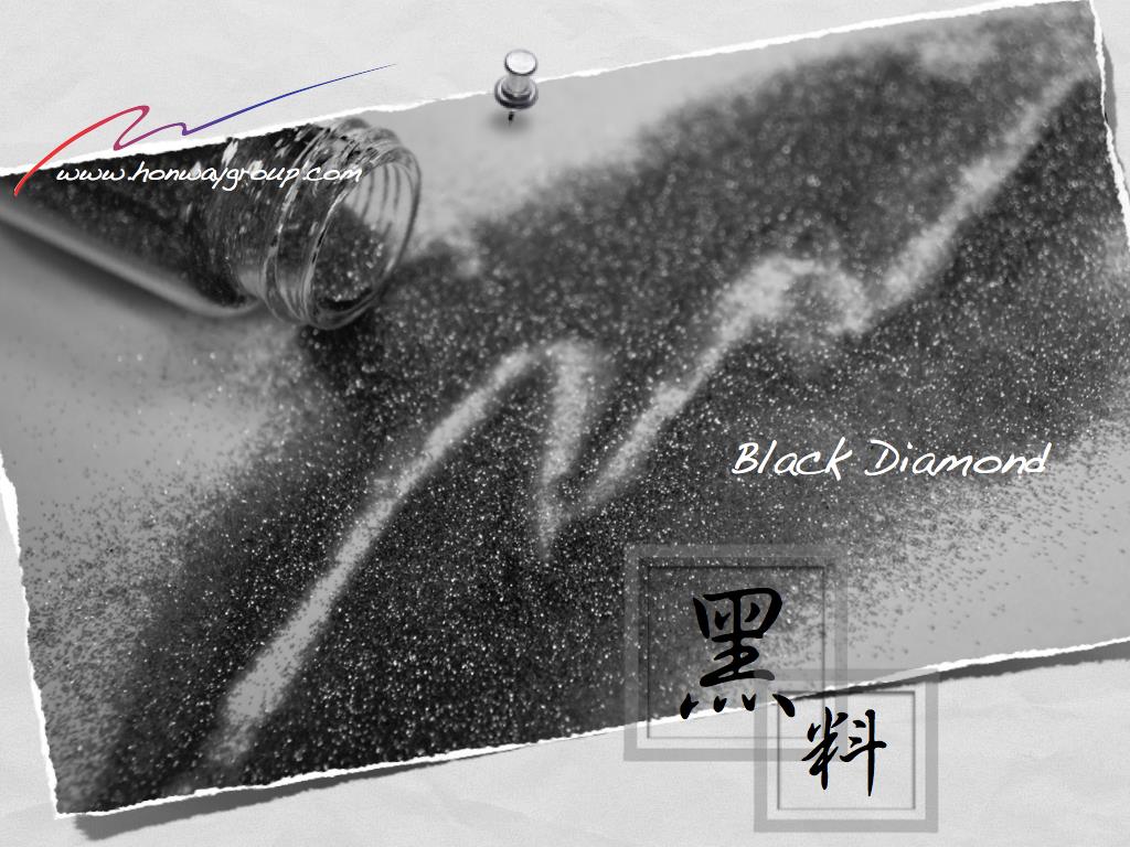
Against this backdrop, diamond heat sinks (diamond substrates) are increasingly seen as the “ultimate material” for solving chip thermal challenges. With an ultra-high thermal conductivity of over 2000 W/(m·K), excellent electrical insulation, and superior mechanical strength, diamond can rapidly disperse hot spots generated during chip operation. This significantly lowers operating temperatures, extends component lifespan, and ensures stable performance. From servers and data centers to aerospace electronics, high-power lasers, and optoelectronic components, diamond is gradually rewriting thermal management standards, becoming an indispensable key material for the semiconductor industry’s move towards higher performance.
Table of Contents
The Unique Advantages of Diamond Substrates: Why They Surpass Traditional Materials
As Moore’s Law progresses, high-power chips are getting smaller, but the heat they generate is constantly increasing. This accumulated heat can form hot spots on the chip, not only affecting performance but even leading to component damage. Diamond substrates provide an ultra-high-speed thermal conduction channel for chips, rapidly dispersing heat and fundamentally solving the hot spot challenge for high-power chips.
Diamond Substrate: A high-performance thermal management material made of diamond, specifically for high-power electronic components and advanced semiconductor devices.
Due to diamond’s extremely high thermal conductivity, it can quickly conduct away the heat generated during component operation, reducing component temperature, and thereby improving performance, stability, and lifespan. As the demand for chip performance continues to increase in fields such as AI, high-performance computing, EVs, and wireless communication, thermal management issues are becoming more severe, and diamond substrates are increasingly seen as the “ultimate material” for solving thermal challenges.
Features of Diamond Substrates

Diamond, due to its multiple superior properties, is hailed as an ideal material for semiconductors:
- Ultra-High Thermal Conductivity: Up to 2000–2400 W/(m·K), far exceeding silicon (150 W/(m·K)) and copper (380 W/(m·K)), enabling rapid dispersion of hot spots.
- Excellent Electrical Insulation: Breakdown field strength can reach 10 MV/cm, suitable for high-voltage, high-power components.
- Wear and Damage Resistance: Extends the lifespan of components and tools, suitable for high-durability applications.
- High Optical Transparency and Low Absorption: Suitable for optical windows, lenses, and high-performance optoelectronic components.
- Strong Chemical Stability: Resistant to acids and alkalis, maintaining stable performance even in harsh chemical environments.
- Good Biocompatibility: Non-toxic and without rejection reactions, applicable in medical devices and implantable devices.
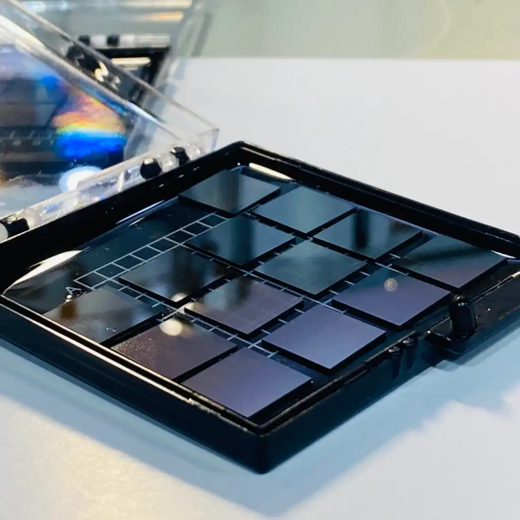
How Are Diamond Substrates Made?
Currently, diamond substrates are primarily manufactured using Chemical Vapor Deposition (CVD). Based on different technological paths, CVD can be divided into the following three main methods:
- Hot Filament CVD
- Method: Uses high-temperature metal filaments to decompose a carbon-containing gas, promoting diamond deposition.
- Features: Stable process, can produce large-area diamonds, relatively low cost.
- Uses: Commonly used for tool coatings and general heat dissipation substrates.
- DC Plasma CVD
- Method: Uses a DC arc to generate high-temperature plasma, rapidly decomposing gases.
- Features: Fast growth rate, can produce diamond structures with extremely high thermal conductivity, close to single crystal.
- Uses: Specifically for high-power density electronic components and optoelectronic heat dissipation substrates.
- Microwave Plasma CVD
- Method: Uses microwave energy to excite high-purity plasma to deposit high-quality diamonds.
- Features: Can produce optical-grade and gem-grade diamonds, with both high thermal conductivity and optical transparency.
- Uses: Widest application range, covering high-power thermal management, medical equipment, optical components, and even jewelry.
Each process has its advantages. Unsure which to choose? Please contact us, and Honway’s experts will provide the most suitable solution for you. Welcome to contact us and let our experts provide you with the most suitable solution.
Physical Properties of Diamond Substrates
Diamond’s material characteristics give it irreplaceable value in the semiconductor industry:
| Grade | Optical Grade | Substrates grade |
| Diamond type | Monocrystalline | Polycrystalline |
| Density | 3.52 g/ cm3 | 3.52 g/ cm3 |
| Raman Full Width at Half Maximum (FWHM) | ~2.1 cm⁻¹ | ~2.85 cm⁻¹ |
| Nitrogen concentration | <0.5 ppm | |
| Thermal conductivity | 1900~2200 W/(m·K) 300K | 1200~2000 W/(m·K) 300K |
| Transmittance | >70% 1064 nm | |
| Index of Refraction | 2.379 @ 10.6 micrometer | |
| Young’s modulus | 850GPa-1200GPa | 850GPa |
| Chemical Stability | Insoluble in all acids and bases | Insoluble in all acids and bases |
| Parallelism | <4μm/cm |
These properties make diamond substrates a core and key material for high-power electronics, optoelectronics, and future nanometer-scale integrated circuits.
Comparison of Single-Crystal and Polycrystalline Diamond
In the application field of diamond heat sinks, CVD diamond is divided into two main categories based on structural differences: monocrystalline and polycrystalline. Different structured CVD diamonds have significant differences in thermal conduction, mechanical strength, optical, and electrical properties, and are therefore applied to different industrial needs. The following table summarizes the main differences between single-crystal and polycrystalline CVD diamond wafers:
| Monocrystalline CVD Diamond Wafer | Polycrystalline CVD Diamond Wafer | |
| Structure | Single, continuous crystal structure | Multiple randomly oriented small crystals |
| Mechanical properties | Excellent hardness, strength and wear resistance | Low strength, affected by grain boundaries |
| Thermal conductivity | Higher, excellent heat dissipation performance | Lower (due to grain boundaries) |
| Optical properties | Exceptional optical clarity and precision | Lower clarity, may have flaws |
| Electrical performance | Highly controllable, direction-dependent | High isotropy, low controllability |
| Application | Electronics, optics, high-performance applications | Industrial tools, radiators, abrasives |
Performance Comparison of Diamond and Other Common Infrared Materials
When selecting semiconductor or optical materials, the differences in physical properties often determine their application range and performance. Especially in high-power electronics, infrared optics, lasers, and precision optical systems, parameters such as bandgap, thermal conductivity, refractive index, and coefficient of thermal expansion directly affect their heat dissipation capabilities, optical performance, and reliability.
| Physical Properties | Unit | Diamond | ZnSe | ZnS | Ge | Si | GaAs | Al₂O₃ | |
| Band gap | eV | 5.48 | 2.7 | 3.9 | 0.664 | 1.11 | 1.42 | 9.9 | |
| Cut-off wavelength | μm | 20 | 14 | 23 | 5.5 | ||||
| Absorption coefficient | 0.1~0.3 | 0.005 | 0.2 | 0.02 | 0.35 | 0.01 | |||
| Absorption coefficient | 10.6 μm | 0.1~0.3 | 0.0005 | 0.2 | 0.2 | ||||
| Microhardness | kg/mm² | 8300 | 137 | 230 | 780 | 1150 | 721 | 190 | |
| Refractive index | 2.38 | 2.40 | 2.19 | 4.00 | 3.42 | 3.28 | 1.63 | ||
| dn/dT | 10⁻³/K | 1.0 | 6.4 | 4.1 | 40 | 13 | 15 | 1.3 | |
| Thermal conductivity | W/(cm·K) | 18~22 | 0.19 | 0.27 | 0.59 | 1.63 | 0.55 | 0.35 | |
| Coefficient of thermal expansion | 10⁻⁶K⁻¹ | Optical Grade | 1.3 | 7.6 | 7.9 | 5.9 | 2.56 | 5.9 | 5.8 |
Honway has compared the key physical properties of diamond with other common materials (such as ZnSe, ZnS, Ge, Si, GaAs, Al₂O₃), demonstrating diamond’s absolute advantage in thermal conductivity, hardness, and optical properties. This explains why diamond can be an ideal material for new-generation heat sinks and optical components.
Diamond vs. SiC/GaN: The Choice of Thermal Management Materials
When selecting thermal interface materials for high-power components, Silicon Carbide (SiC) and Gallium Nitride (GaN) are common options, but when faced with more severe hot spot challenges, diamond stands out due to its ultra-high thermal conductivity.
We provide you with a comparison of diamond vs. SiC for heat dissipation to help you make the best technical choice.
| Characteristics | Diamond | Silicon Carbide (SiC) |
| Thermal Conductivity | 1,200 – 2,200 W/(m·K) | About 150 – 200 W/(m·K) |
| Thermal conductivity | Extremely high, it is the best among currently known materials and can quickly disperse hot spots. | Good, far superior to traditional silicon, suitable for medium to high power applications. |
| Electrical Insulation | Excellent, with a breakdown electric field strength of 10 MV/cm. | Excellent, with a breakdown electric field strength of 3 MV/cm. |
| Physical properties | High hardness, wear resistance and excellent chemical stability. | High hardness, wear resistance, high temperature and high pressure resistance. |
| Material costs | The initial cost is higher, but it can bring higher performance and lifespan. | It is relatively low compared to diamonds and is widely used in the mainstream market. |
| Application Scenario | High-performance computing (HPC), data center servers, aerospace electronics, high-power lasers, and other extreme applications with extremely high thermal management requirements. | Medium and high power electronic devices such as electric vehicle inverters, charging stations, 5G base stations, and power supplies. |
How to choose:
Choose Diamond: If your project’s core goal is to pursue ultimate performance, highest reliability, and the longest component life, and you are facing difficult-to-solve hot spot issues, then diamond substrates are your ultimate solution. They allow chips to run stably at higher frequencies and break through the performance bottlenecks of traditional materials.
Choose SiC: If the product you are developing falls into the mainstream mid-to-high-power applications and you hope to strike a balance between performance and cost, then SiC is still an excellent and highly competitive material.
The Investment Benefits of Diamond Substrates
Many customers, when evaluating diamond wafers, are most concerned about their cost.
Although the initial investment is higher, from a long-term perspective, the performance improvement and extended component life brought by diamond substrates can significantly reduce the overall system’s operating and maintenance costs.
For high-end applications that pursue ultimate performance, the return on investment far exceeds that of traditional materials.
Application Fields of Diamond Substrates
With its superior thermal conductivity, electrical insulation, and mechanical strength, diamond substrates exhibit immense value in multiple advanced technology fields, becoming a key material supporting new-generation high-performance devices.
- Thermal Interface Materials (TIMs): Diamond wafers can be used as a highly efficient thermal interface layer between chips, modules, and heat sinks, effectively reducing thermal resistance, significantly improving thermal conduction efficiency, and ensuring the stable operation of high-power components.
- Electronic Packaging and Substrates: In semiconductor packaging, diamond substrates provide excellent heat dissipation performance, supporting components to operate for extended periods under high power density, driving the development of electronic products towards miniaturization and high performance.
- Servers and High-Performance Computing: Diamond can be used as a heat spreader for high-power crystals such as GaN and SiC, reducing internal temperature rise and extending component life, improving the stability and reliability of data center and server systems. Its excellent high-temperature resistance and mechanical properties are also very suitable for advanced packaging technologies such as 2.5D/3D stacking.
- LED and Optoelectronic Components: In the fields of LEDs and optoelectronics, diamond substrates can significantly improve thermal management, extend component life, and enhance luminous efficiency and brightness, meeting the stringent requirements of high-end optoelectronic applications.
- Insulation Substrates: CVD diamond wafers, with their high thermal conductivity and excellent electrical insulation, can serve as ideal insulating substrates for power electronic components an
- Medical Devices: Industrial diamonds are also widely used in the medical field, for example, in high-precision surgical instruments and dental drills. Their high hardness and wear resistance significantly improve the life and precision of medical tools.
More Information on Honway Diamond Grinding and Polishing Consumables:
To learn more about how Honway can bring breakthrough benefits to your semiconductor processes, please click the links below to explore our full range of diamond grinding and polishing consumables and technical details:
- Honway Nanodiamond Polishing Liquid Series
- Honway Precision Wafer Grinding and Polishing Pads
- Honway Grinding Wheels for Wafer Surface Grinding
- Honway Chamfering and Grinding Wheels for Silicon Wafers
- Honway Wafer Electroplated Dicing Blade
- Honway Wafer Packaging Dicing Blade – Soft Blade
- Honway Wafer Packaging Dicing Blade – Hard Blade
- Honway Diamond Substrates
You can also directly “contact our Honway expert team,” and we will provide the most professional customized consultation and solutions.
Frequently Asked Questions (FAQ)
- Q1: Is the cost of diamond heat dissipation substrate high?
- A: The initial cost of a diamond substrate is indeed higher than traditional materials. However, for applications that demand high stability, long lifespan, and extreme performance (such as high-performance computing, aerospace, or military), its superior thermal management capabilities can extend component life and improve system stability. In the long run, this significantly reduces the total cost of ownership. We would be happy to discuss a specific return-on-investment analysis with you.
- Q2: Can CVD diamond be used in 2.5D/3D packaging?
- A: Yes. The excellent thermal conductivity and mechanical strength of CVD diamond make it an ideal choice for 2.5D/3D packaging technology. In advanced packaging, a diamond substrate can serve as a critical heat spreader, effectively managing the heat generated by vertically stacked chips to ensure the reliability of heterogeneous integration and high-density packaging. This is one of the core application areas of our Honway technology.
- Q3: How long is the supply cycle for your diamond wafers?
- A: Our supply cycle is determined by your customization needs, such as size, grade, and quantity. Please contact our expert team directly, and we will provide the most accurate quotation and delivery time estimate based on your project requirements.
- Q4: Besides heat dissipation, what other advantages does diamond have for applications?
- A: In addition to thermal conductivity, diamond also possesses excellent electrical insulation and chemical stability. This makes it an ideal insulating substrate for power electronic components and high-frequency radio frequency (RF) devices. Furthermore, its high hardness and wear resistance are also widely applied in precision grinding and medical equipment fields.
Read More Related Topics
- Diamond Substrate>>>From jewelry to semiconductors: Diamonds play a key role in the next generation of thermal conductivity materials
- Compound Semiconductors>>>The secret weapon of semiconductor precision manufacturing: diamond grinding and polishing consumables, effectively improving wafer yield and performance!
- Semiconductor grinding and polishing>>>Grinding and Polishing in Semiconductor Manufacturing: Excellence from Material Selection to Consumable Empowerment
- Grinding and polishing cunsumbles>>>Innovative Grinding and Polishing Consumables: Driving the Semiconductor Industry Towards Higher Precision
- The key to ultra-flat wafers>>>The “Thin” Science of Semiconductor Grinding and Polishing: Key to Achieving Ultra-Flat Wafers
- Heterogeneous Integration and Advanced Packaging>>>Facing the Future: How Grinding and Polishing Consumables Empower Heterogeneous Integration and Advanced Packaging
- Polerowanie półprzewodników złożonych>>>Mastering Compound Semiconductor Polishing Technology: Achieving High Performance for Next-Generation Electronic Components
- Silicon carbide and gallium nitride>>>Focusing on SiC and GaN: Breakthroughs and Challenges in Compound Semiconductor Grinding and Polishing Technology
We offer customized adjustments to the grinding process, tailored to meet processing requirements for maximum efficiency.
After reading the content, if you still don’t know how to select the most suitable option,
Feel free to contact us and we will have specialist available to answer your questions.
If you need customized quotations, you’re also welcome to contact us.
Customer Service Hours: Monday to Friday 09:00~18:00 (GMT+8)
Phone: +8867 223 1058
If you have a subject that you want to know or a phone call that is not clear, you are welcome to send a private message to Facebook~~
Honway Facebook: https://www.facebook.com/honwaygroup
You may be interested in…
[wpb-random-posts]