In high-tech sectors such as 5G communications, electric vehicles (EVs), laser systems, and quantum computing, the power density of electronic components is increasing at an unprecedented rate. The resulting massive thermal flux has become a critical bottleneck restricting device performance, reliability, and operating lifespan. Traditional thermal interface and substrate materials—such as copper, aluminum, aluminum nitride (AlN), and silicon carbide (SiC)—are reaching their physical limits when handling extreme heat loads.
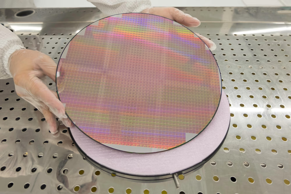
Against this backdrop, synthetic industrial diamond—specifically high-purity CVD Diamond Substrates manufactured via Chemical Vapor Deposition—has emerged as the ultimate high-power thermal management solution, leveraging its unparalleled physical properties.
1. Comparative Analysis: Hot-Filament, DC Plasma, and Microwave CVD
CVD diamond production involves decomposing carbon source gases (such as methane) under controlled conditions, enabling carbon atoms to deposit into a crystalline diamond structure. Several distinct synthesis techniques are utilized, each resulting in different diamond quality, scalability, and cost profiles:
| CVD Method | Mechanism & Characteristics | Quality & Thermal Conductivity | Primary Applications |
|---|---|---|---|
| Hot-Filament CVD (HFCVD) | Decomposes gas using high-temperature tungsten filaments. Cost-effective for large-area deposition. | Lower purity due to tungsten filament contamination and lower plasma density; limited thermal conductivity. | Tool coatings and basic industrial thermal management. |
| DC Plasma Jet CVD (DC-PACVD) | Utilizes direct current arc discharge to generate plasma. Higher plasma density and gas decomposition rate. | Better quality and faster growth rates than HFCVD; challenges remain in large-area uniformity and purity control. | Bulk diamond deposition and medium-to-high load thermal sinks. |
| Microwave CVD (MWCVD) | Generates electrodeless plasma via microwave energy. Eliminates electrode contamination and enables precise impurity control. | Highest purity, lowest defect density, and superior electrical properties approaching natural diamond. | Electronic-grade thermal substrates, RF power devices, and optical windows. |
2. Applications of Optical-Grade and Gem-Grade High-Quality Diamond
High-quality CVD diamond can be categorized into various grades based on purity, defect density, and optical scattering, each serving specific industry applications:
- Gem Grade: Focuses primarily on color, clarity, and carat weight for the jewelry market. Thermal conductivity typically ranges from 1,000 W/mK up to natural diamond levels of ~2,200 W/mK.
- Optical Grade: Engineered for extremely low impurities and minimal light scattering, requiring exceptional optical transparency. Due to high purity, its thermal conductivity is extraordinarily high. It is widely used in high-power laser windows and lenses to rapidly conduct heat away from intense laser beams and prevent thermal lens distortion.
- Electronic Grade (Thermal Management Grade): A refined subset of optical grade, specifically optimized for ultra-low impurities (such as nitrogen and boron) and high crystal perfection to maximize phonon thermal transport. These high-purity substrates are designed for demanding electronic heat dissipation, including high-power RF amplifiers and high-voltage power devices.
3. Enhancing Electronic Component Performance and Lifespan
Diamond possesses the highest thermal conductivity of all known solid materials (exceeding 2,000 W/mK at room temperature—more than 5 times that of copper) alongside excellent electrical insulation. Integrating Hon Way’s diamond substrates into high-power semiconductor packaging converts these physical advantages into measurable system upgrades:
- Extreme Thermal Conduction & Spreading: Bonding or growing diamond substrates directly beneath semiconductor dies (e.g., high-frequency GaN-on-Diamond chips) serves as an ideal heat spreader. It instantly draws heat away from local hotspots, substantially reducing junction temperature (Tj).
- Significant Increase in Power Density: Lower junction temperatures allow chips to operate safely at higher power levels, currents, and frequencies. For RF power amplifiers in 5G base stations and phased-array radar, diamond substrates significantly boost output power and linearity.
- Extended Component Lifespan & Reliability: Semiconductor degradation typically follows the Arrhenius law—a 10°C drop in junction temperature can double device operational reliability. Superior thermal dissipation radically reduces thermal stress and operating temperatures, ensuring long-term system stability.
- Enabling System Miniaturization: Enhanced thermal efficiency enables the use of smaller semiconductor dies, more compact thermal cooling designs, or reduced cooling power requirements—critical advantages for EV inverters and aerospace applications.
4. Hon Way Materials: Customized Top-Tier Thermal Material Solutions
CVD diamond substrates are rapidly becoming the cornerstone of next-generation high-power electronics. However, diamond’s extreme hardness presents significant challenges during surface processing. Achieving perfect wafer-level bonding yields requires ultra-precise grinding, polishing, and surface roughness control techniques to eliminate microscopic voids and fully realize its thermal potential.
With extensive expertise in high-purity semiconductor materials and consumable supply, Hon Way Materials introduces high-specification electronic and optical-grade diamond substrates and diamond wafers for advanced semiconductor processes. Whether you require custom dimensions, tailored thicknesses, or a comprehensive thermal management architecture, Hon Way offers flexible, technically advanced local support commitments.
Contact Hon Way Technical Experts
Looking to unlock the full performance potential of your production line, or currently facing critical chip overheating bottlenecks? Hon Way Materials is your trusted R&D partner for high-power thermal management solutions.
Submit RFQ / Contact Hon Way Directly →