
With China implementing export controls on specific industrial diamond products on November 8, the global high-precision manufacturing industry—especially in semiconductors and high-power components—faces the risk of supply chain disruption.
At this critical moment, Honway Industrial, with **sufficient stock in Taiwan** of **Diamond, Alumina, and CBN abrasives and consumables**, offers you a **stable, high-quality alternative supply solution**.
This article will explore high-end applications of industrial diamonds in semiconductors and heat dissipation, demonstrating how Honway can be your key partner in navigating supply chain challenges.
Table of Contents
Core Characteristics of Diamond
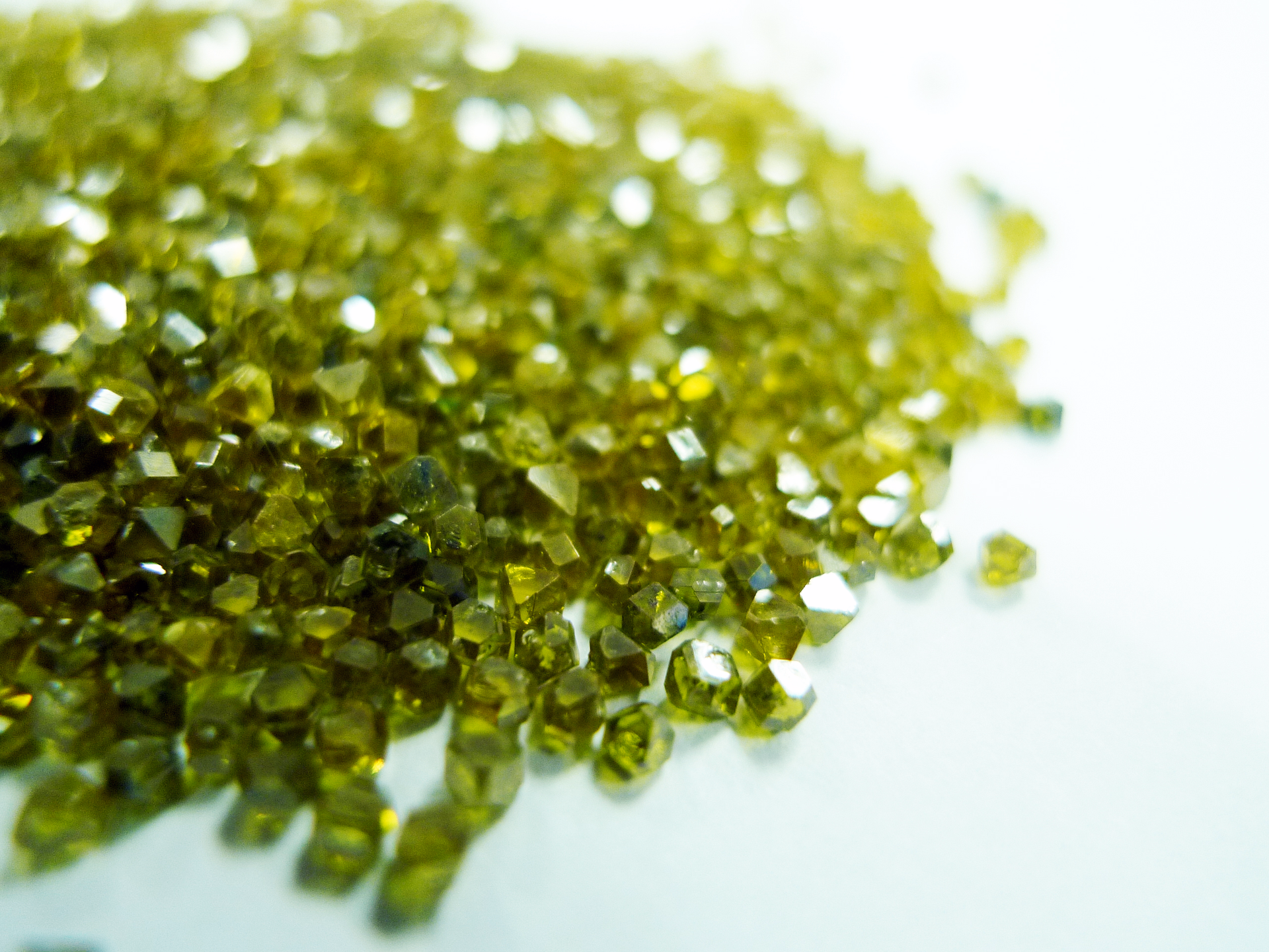
Diamond is a crystalline form of carbon and an allotrope of carbon, like graphite. Its chemical composition is almost pure carbon, containing only trace amounts of nitrogen impurities (about 0.01–0.25%). Pure diamond is transparent and colorless; however, due to impurities or lattice defects, it may appear in various shades such as pale yellow, blue, or green. Generally, natural diamonds are often pale yellow, while synthetic diamonds frequently exhibit a yellow-green appearance.
In terms of physical properties, diamond possesses:
- The highest hardness of any known material (Mohs hardness of 10), with a density of approximately 3.515 g/cm³.
- Extremely high thermal conductivity (approx. 2200–2600 W/m·K).
- Excellent electrical insulation and chemical stability. Its surface is hydrophobic and lipophilic, extremely inert at room temperature, and resistant to corrosion by general chemical reagents.
Under oxidizing conditions, diamond stability varies with the environment: above 600°C in pure oxygen, the surface gradually loses luster and blackens; combustion begins between 700–800°C. The oxidation onset temperature for synthetic diamonds is approximately 740–840°C, with combustion temperatures falling between 850–1000°C.
With its **extreme hardness, excellent thermal conductivity, optical transparency, and high sound velocity propagation**, diamond can operate stably in extreme high-temperature, high-pressure, and highly corrosive environments, making it the ideal choice for **high-precision machining, thermal management components, and advanced semiconductor materials**.
Diamond Thermal Conductivity Mechanism and Electronic Application Potential
Diamond’s heat conduction relies mainly on the **phonon transfer mechanism**. Due to its tight lattice, strong covalent bonds, and minimal defects, phonons can propagate at high speeds with little scattering, forming excellent thermal conduction channels.
In high-power chips, reliability drops by about 10% for every 1°C rise in temperature.
Diamond substrates effectively disperse heat, suppress hotspots, and enhance system stability, making them the core material for next-generation power chips and high-efficiency cooling solutions.
Industrial Applications of Diamond
1. Precision Cutting and Ultra-Mirror Polishing
Diamond abrasives, with their unrivaled hardness, are the top choice for processing various super-hard and brittle materials. This application field spans traditional manufacturing, precision optics, and medicine, ensuring products meet the highest standards of geometric precision and surface finish.
- Traditional Industry and Molds: Precision grinding, polishing, and sharpening of hard alloys (e.g., Tungsten Carbide), ceramics, and mold steels.
- Precision Optics and Chemistry: Fine grinding and polishing of sapphire substrates, optical glass, quartz, and fiber optic ends, as well as chemical instrument applications like diamond electrodes and diamond-coated tools.
- Medical and Structural Ceramics: Precision forming of biomaterials like bio-ceramics, high-strength ceramic dentures, and artificial joints.
Honway: Sufficient Spot Stock, General Abrasives, and Consumables Supply List
To cope with the impact of China’s controls, Honway provides sufficient stock to ensure uninterrupted customer production lines:
- Full Grit Size Abrasive Supply: Diamond abrasives ranging from **#60 (coarse grinding)** to micron level, as well as single-crystal and polycrystalline **micron-level polishing powders**, meeting needs from coarse grinding to ultra-precision polishing.
- Diverse Grinding Media: High-performance **Alumina** and **CBN (Cubic Boron Nitride) abrasives**, customizable according to workpiece material characteristics.
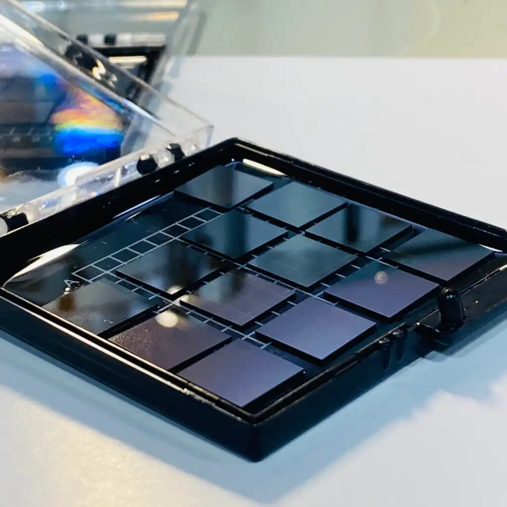
Cutting and Forming Tools: Various precision cutting, forming wheels, and **semiconductor dicing blades** (for wafers and hard/brittle materials).
2. High-End Semiconductor Solutions: SiC/GaN CMP Process and Diamond Heat Dissipation Substrates
As power density in AI servers, 5G, and EVs climbs sharply, thermal management and process yield have become the biggest bottlenecks for chip reliability. Diamond plays a dual role in advanced semiconductors, evolving from a “tool” to a “critical material.”
A. Wafer-Level Precision Process: Compound Semiconductor CMP Projects
In the manufacturing of advanced semiconductors (especially compound semiconductors like SiC, GaN, Ga2O3), CMP (Chemical Mechanical Polishing) is a critical step determining yield and performance. Traditional abrasives struggle to meet SiC/GaN requirements for **nanometer-level flatness** and **low sub-surface damage (SSD)**.
Honway CMP Solutions: Diamond polishing slurries and precision polishing pads designed specifically for SiC, GaN, and AlN.
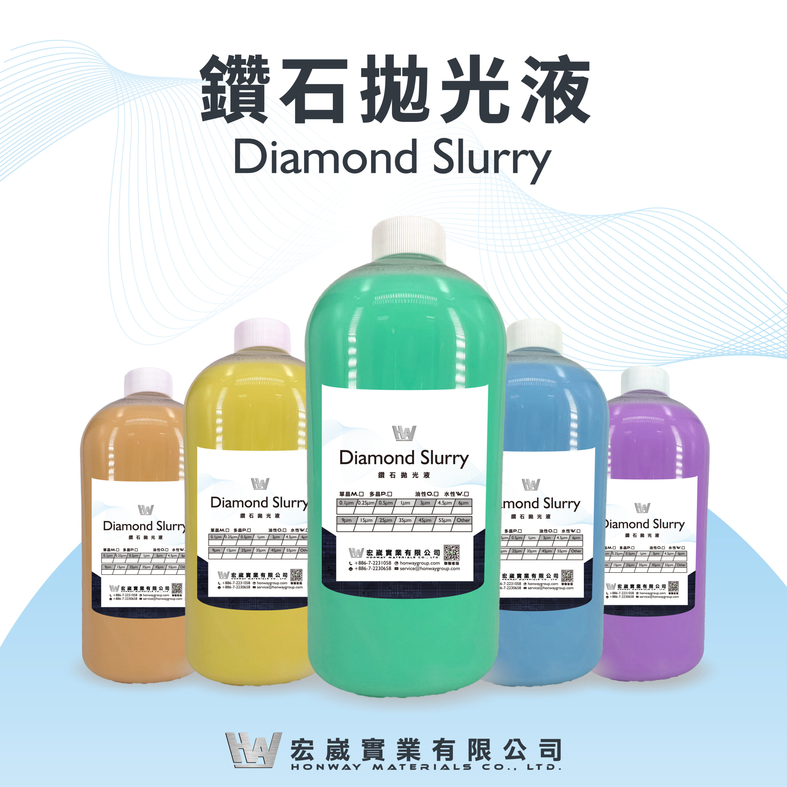
Specialized Diamond Slurry: Introduces surface microstructure optimization and spherical diamond particles to achieve damage-free polishing for SiC/GaN. Provides high-purity diamond micropowder and precision dispersion technology, meeting single/polycrystalline polishing needs from **#60 to nanometer level**.
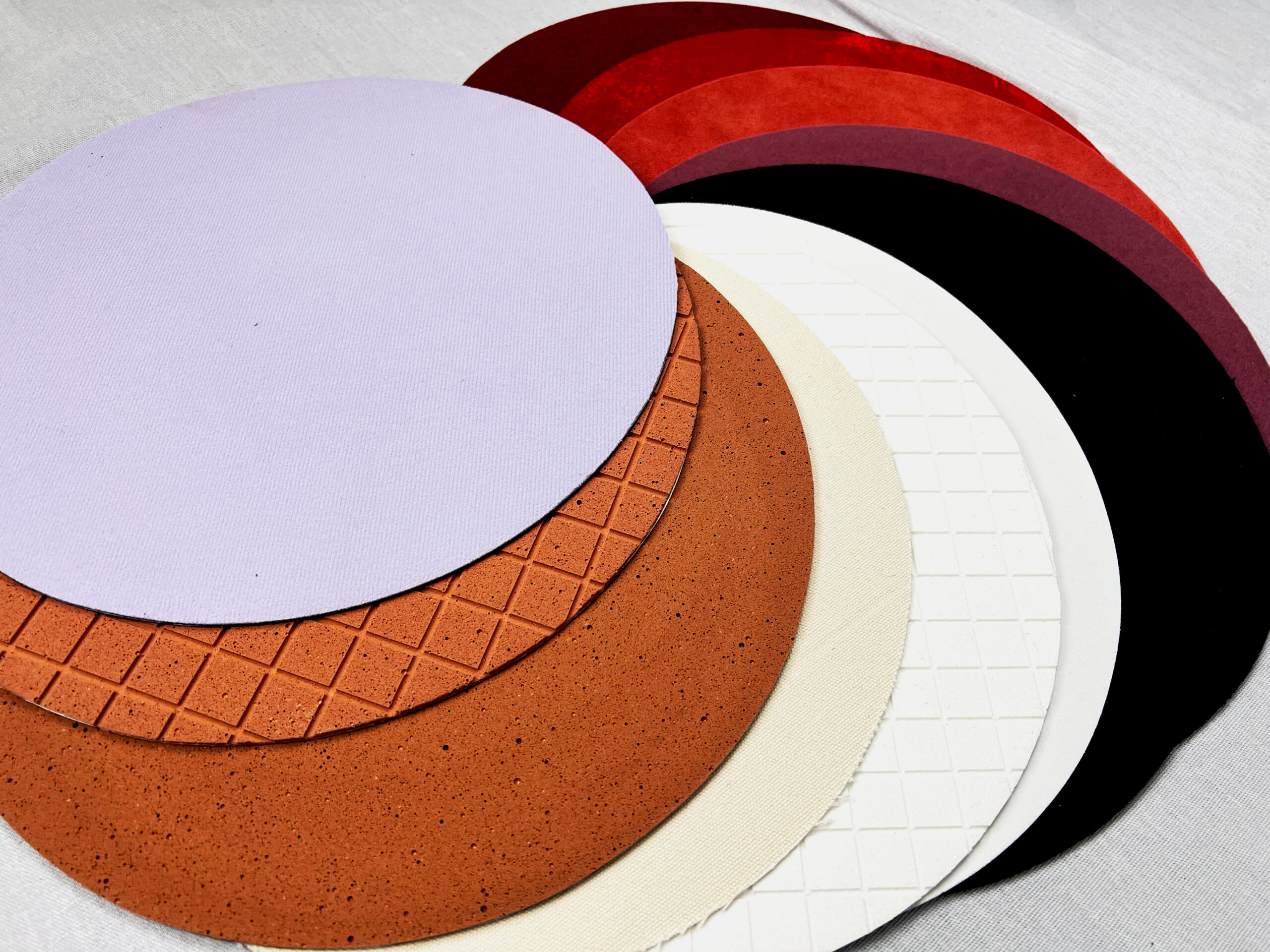
Precision Polishing Pad Series: Features high mechanical stability and chemical resistance, suitable for materials like SiC, GaN, sapphire, and optical glass, enhancing throughput and surface consistency.
Customization Advantage: Polishing parameters can be fine-tuned according to different substrate hardness and chemical properties, offering precise chemical reaction control.
B. Thermal Material Innovation: Diamond Substrates Spot Supply
With its dual advantages of **extremely high thermal conductivity (approx. 2200 W/m·K)** and **excellent electrical insulation**, diamond has become the top choice for heat dissipation substrates in next-generation power components.
- Value of Diamond Heat Sinks: Effectively reduces chip operating temperature by 20–30%, extends component life, and supports high power density and high-frequency heterogeneous integration packaging.
Honway Spot Supply: Honway maintains **spot stock of diamond heat dissipation substrates**, helping customers bypass supply chain bottlenecks and quickly implement diamond thermal solutions into high-power lasers, RF modules, and power management chips.
3. Precision Optics, Medical, and Chemical Applications
- Optical Components: Diamond’s high transparency and excellent wear resistance make it suitable for infrared windows and laser optical components.
- Chemistry and Instruments: Diamond electrodes and diamond-coated tools remain stable in highly corrosive and high-temperature environments, used in chemical reactors, diamond substrates, and sensors.
Current Market Size of Diamond
| Application Area | 2025 Market Size (USD) | Projected CAGR | Key Industries |
| CVD Diamond Submounts | 13.6 Billion | 11.7% (2024–2031) | High-power semiconductors, Lasers, Comm modules |
| Diamond Heat Spreaders | 180 Million | 9.86% (2025–2033) | Aerospace, Defense, Telecom, Advanced Electronics |
| Diamond Heat Sinks | 240 Million | 4.2% (2025–2033) | High-power electronics, Optical modules |
| Cu-Diamond Composites | 338 Million | 12.1% (2025–2033) | HPC, 5G, EV, Aerospace |
| Single Crystal Diamond Market | 1.637 Billion | 4.7% (2025–2033) | Precision tools, Semiconductors, Optics |
Market Growth Drivers
- High Power Density Electronic Devices: With the development of semiconductors, 5G, Electric Vehicles (EV), and AI servers, the demand for efficient thermal management materials is increasing daily.
- Advances in CVD Technology: The maturity of Chemical Vapor Deposition (CVD) technology has made mass production of high-quality diamond materials possible, reducing costs and expanding the range of applications.
Conclusion
Diamond is no longer just jewelry; it is a core material driving technological evolution. From wafer planarization and power component heat dissipation to high-precision optical machining, diamond plays an irreplaceable role across industries. Honway, with deep material technology and application experience combined with innovative grinding and polishing solutions, is leading diamond materials onto a broader high-tech application stage.
However, with China’s recent implementation of export controls on specific synthetic diamond products and related process equipment… choosing a reliable industrial diamond partner and advanced technology not only ensures continuous production stability but also maintains a competitive edge amidst global supply chain shifts. The value of diamond is extending from the “material itself” to “industrial strategy” and “technological mastery.”
Act Now! Due to surging market demand, please **contact our Honway expert team immediately**.
We will provide you with customized **spot supply solutions** for SiC/GaN and optical materials, along with the most professional process consultation.
More Honway Diamond Polishing Consumables Information
To learn more about how Honway can bring breakthrough benefits to your semiconductor process, please click the links below to explore our full range of diamond grinding and polishing consumables and technical details:
- Honway Nano Diamond Polishing Slurry Series
- Honway Precision Wafer Polishing Pads
- Honway Wafer Surface Grinding Wheels
- Honway Silicon Wafer Chamfering Wheels
- Honway Wafer Electroformed Dicing Blades
- Honway Wafer Packaging Dicing Blades – Soft
- Honway Wafer Packaging Dicing Blades – Hard
- Honway Diamond Heat Dissipation Substrates
You can also directly “Contact Our Honway Expert Team” for the most professional customized consultation and solutions.
Read More Related Topics
- Diamond Substrates >>> From Jewelry to Semiconductors: Diamond Becomes Key to New Generation Thermal Materials
- Compound Semiconductors >>> Secret Weapon of Precision Semiconductor Manufacturing: Diamond Polishing Consumables
- Semiconductor Polishing >>> Polishing in Semiconductor Manufacturing: Excellence from Material Selection to Consumable Empowerment
- Polishing Consumables >>> Innovative Polishing Consumables: Driving the Semiconductor Industry to Higher Precision
- Key to Ultra-Flat Wafers >>> The “Thin” Science of Semiconductor Polishing: Key to Achieving Ultra-Flat Wafers
- Heterogeneous Integration & Advanced Packaging >>> Facing the Future: How Polishing Consumables Aid Heterogeneous Integration and Advanced Packaging
- Compound Semiconductor Polishing >>> Mastering Compound Semiconductor Polishing Technology: Achieving High Efficiency for Next-Gen Electronics
- SiC & GaN >>> Focus on SiC and GaN: Breakthroughs and Challenges in Compound Semiconductor Polishing Technology
- Diamond Export Controls >>> China Implements Synthetic Diamond Export Controls: Global Supply Chains and Taiwan Industry Face New Challenges
- Diamond >>> Abrasives – Diamond Introduction
Regarding polishing, we offer customized adjustments, modifying ratios according to processing needs to achieve maximum efficiency.
If you are still unsure how to select the most suitable product after reading this.
Please feel free to contact us; our specialists are ready to answer your questions.
Contact us if you need a quotation for custom orders.
Customer Service Hours: Mon-Fri 09:00~18:00
Tel: +886 7 223 1058
If you have topics you’d like to understand or can’t clarify over the phone, feel free to message us on Facebook!
Honway Facebook: https://www.facebook.com/honwaygroup
You might be interested in…
[wpb-random-posts]