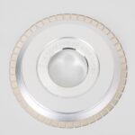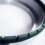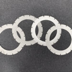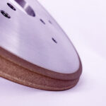
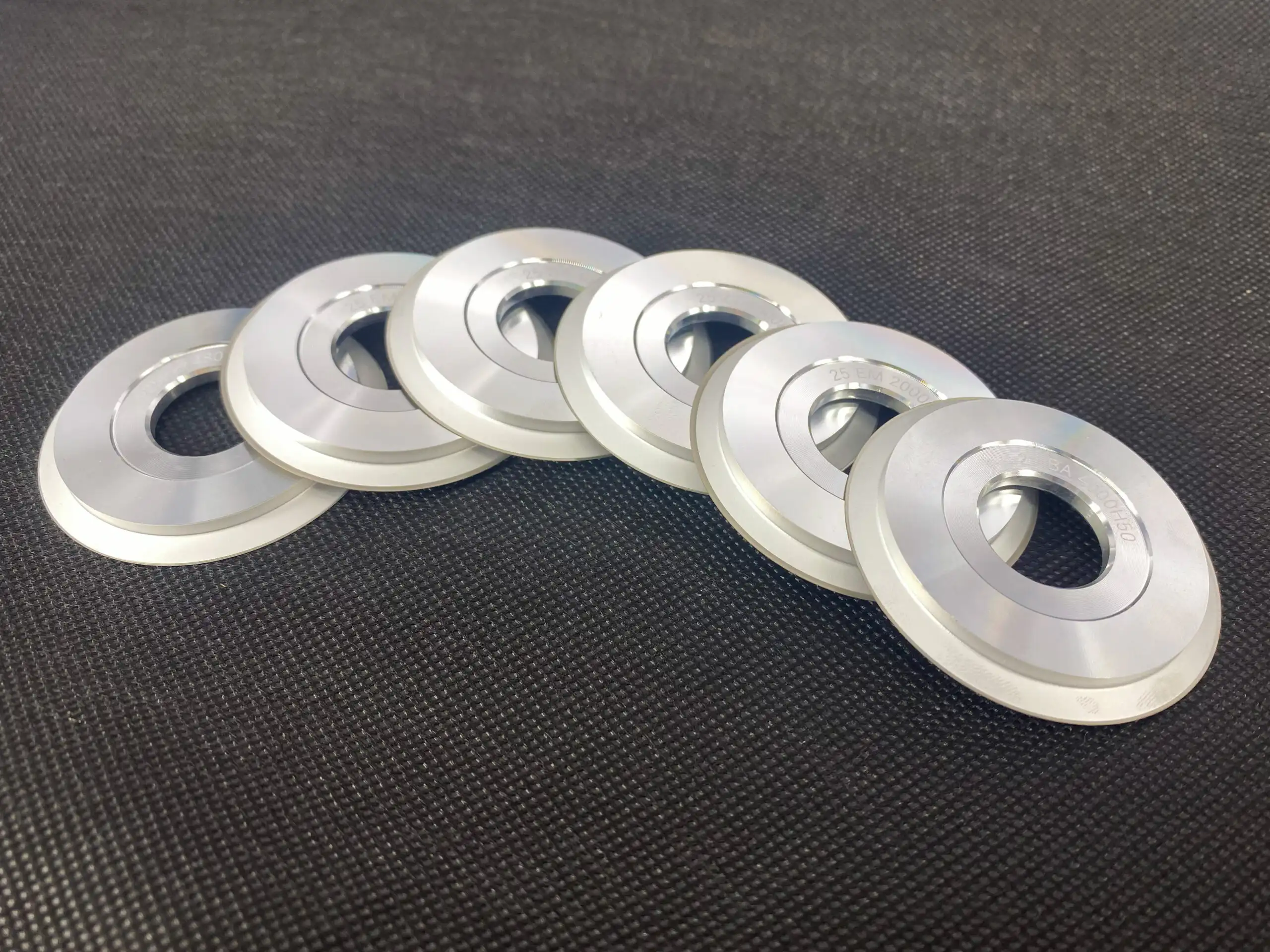
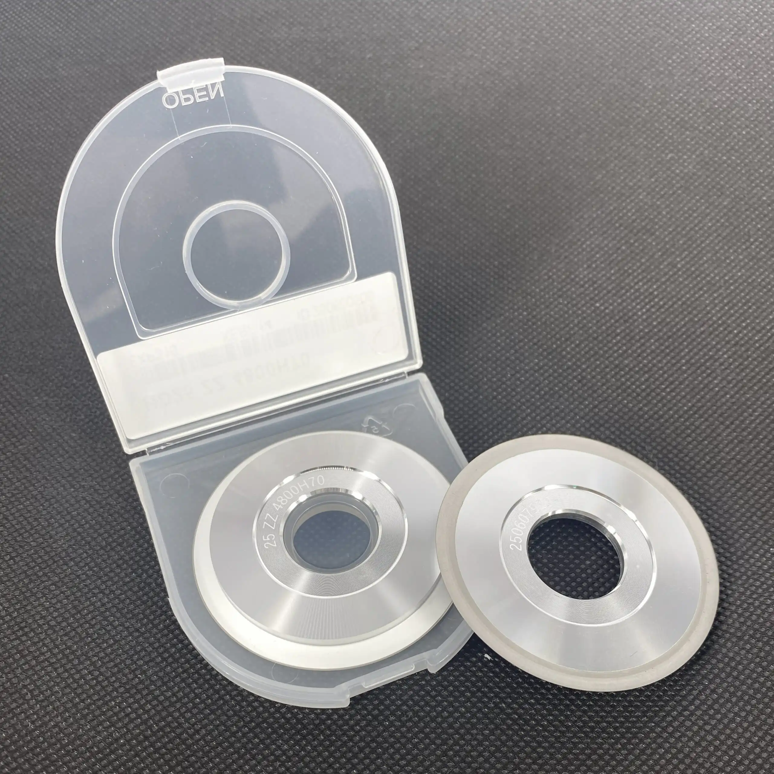

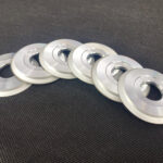
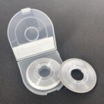
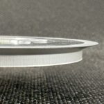
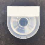
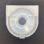
HWD25 Wafer Eletroplated Dicing Blade
Honway Materials provide customized services,
Make the most suitable wafer electroplated dicing blade for you
It is suitable for processing semiconductor wafers, packaging substrates and various hard and brittle materials such as LTCC, PZT, TGG, etc.
Product Features:
- High Precision Machining Capability: Adopts a high-rigidity electroplated structure and strictly controlled blade geometry to ensure a stable and consistent cutting line width, achieving high-precision, high-yield micron-level processing.
- Ultra-Narrow Kerf Design: Ultra-narrow kerf width, with a minimum of 10 μm, meets the dicing needs of high-density layouts and narrow streets on wafers like GaAs LEDs, improving wafer utilization and reducing material loss.
- Suitable for Various Wafer Materials: Including monocrystalline silicon, oxide wafers such as silicon dioxide and silicon nitride, and III-V compound semiconductors such as silicon carbide (SiC), gallium arsenide (GaAs), and gallium phosphide (GaP).
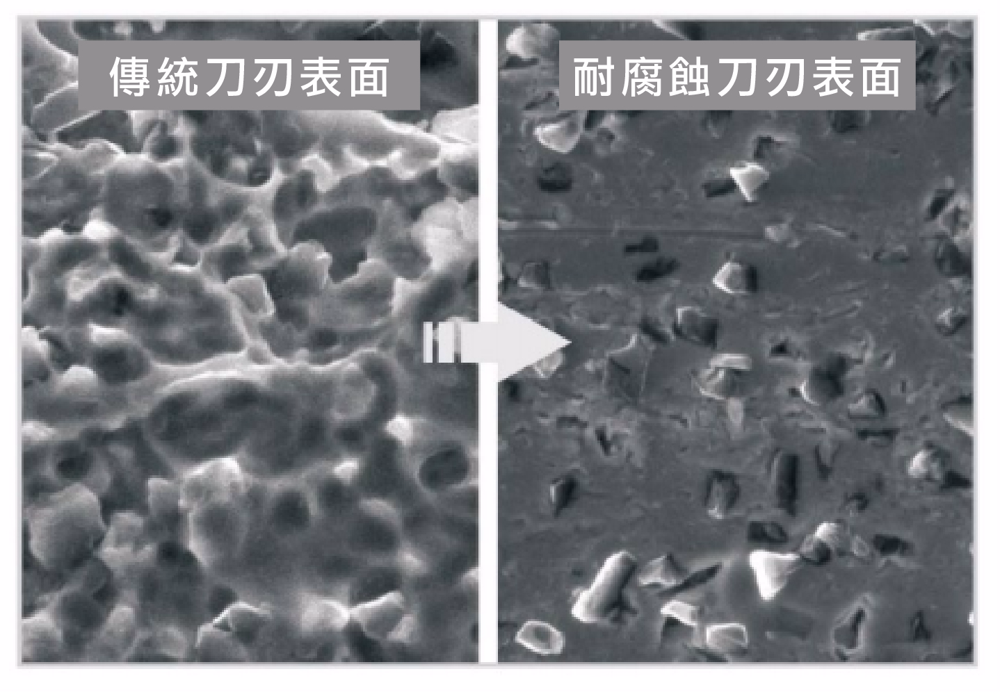
- Excellent Blade Life and Stability: The blade has excellent chemical stability, effectively resisting corrosion risks in wet or CO₂-assisted cutting environments, significantly extending blade life.
- Ultra-Narrow Diamond Micro-Powder Particle Size Distribution, Paired with Highly Consistent Crystal Shape Selection: Carefully selected high-compactness diamond crystal shapes with a uniform particle size distribution ensure the cleanliness of the machined surface and cutting stability, improving finished product yield.
- High Blade Strength and Rigidity Design: Suitable for high-speed operation environments, it can effectively prevent offset phenomena like “snake marks” during cutting, while ensuring good perpendicularity and neatness of the die sidewalls.
- Customizable Blade Specifications: Provides different blade thicknesses, outer diameters, blade shapes, and metal matrix hardness to meet various wafer sizes and cutting needs.
Uses:
- Suitable for cutting or grooving, especially for wafer dicing and semiconductor packaging.
- Used during the semiconductor wafer dicing process stage.
Application areas:
- Suitable for the precision cutting and processing of silicon wafers, oxide wafers, and various compound wafers such as silicon carbide (SiC), gallium arsenide (GaAs), and gallium phosphide (GaP).
- Composite silicon wafers, electronic materials, resins, metals, ceramics, composite materials, etc.
Please specify the following when ordering dicing blades:
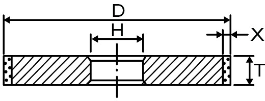
- Shape and dimensions of the dicing blade:
- Blade protrusion amount (um): For example, Z(250-380)
- Kerf width: For example, A(16-20)
- Grit size: For example, #1800
- Bond type: For example, N general-purpose
- Concentration: For example, 90
- Use: For silicon carbide (SiC), gallium arsenide (GaAs), gallium phosphide wafers
- Quantity and delivery time:
- RPM and processing conditions:
- Processing equipment model:
- Most manufacturers mark the following information on the dicing blades, with a specification example: CB 3000N70
| Blade Exposure (µm) | Kerf Width (µm) | Particle Size | Binder | Concentration (Volume) |
| Z 250-380
A 385-510 B 510-640 C 640-760 D 760-890 E 890-1020 F 1020-1150 G 1150-1270 |
Z 11-15
A 16-20 B 20-25 C 25-30 D 30-35 E 35-40 F 40-50 G 50-60 |
#1000
#1500 #1700 #1800 #2000 #2500 #3000 #3500 #4000 #4500 #4800 #5000 |
S Sharp Type
N General Type H High Strength Type |
50
70 90 110 130 |
Sample images:
Product technical advantages:
Carefully selected high-compactness diamond crystal shapes and uniform particle size distribution ensure the cleanliness of the machined surface and cutting stability, improving finished product yield.
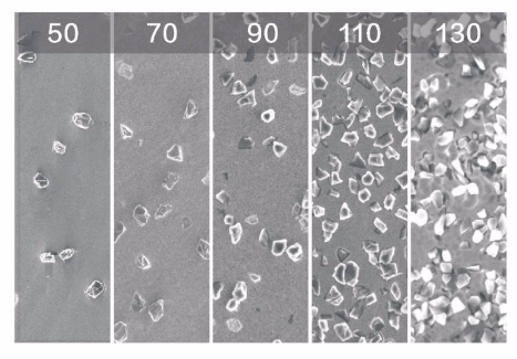
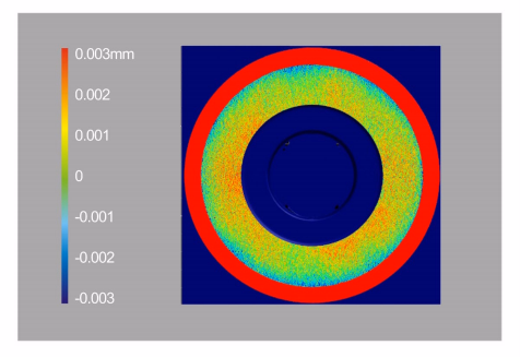
By precisely controlling the diamond concentration, the HWD25 series effectively balances processing stability and tool life, showing excellent performance in reducing wafer backside chipping to achieve high-yield, high-reliability cutting results.
The high-precision process can reduce adjustment and pre-calibration time before cutting, while effectively reducing blade runout and vibration during high-speed operation, enhancing machine stability.
The blade possesses excellent chemical stability, effectively resisting corrosion risks in wet or CO₂-assisted cutting environments, significantly extending blade life.
The ultra-narrow kerf width, with a minimum of 10 μm, meets the dicing needs of high-density layouts and narrow street wafers like GaAs LEDs, improving wafer utilization and reducing material loss.
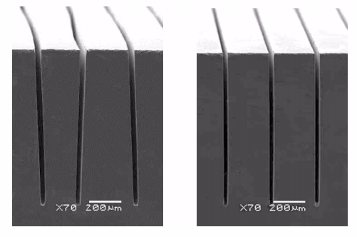
Suitable for high-speed operation environments, it can effectively prevent offset phenomena like “snake mark.
Use Case:
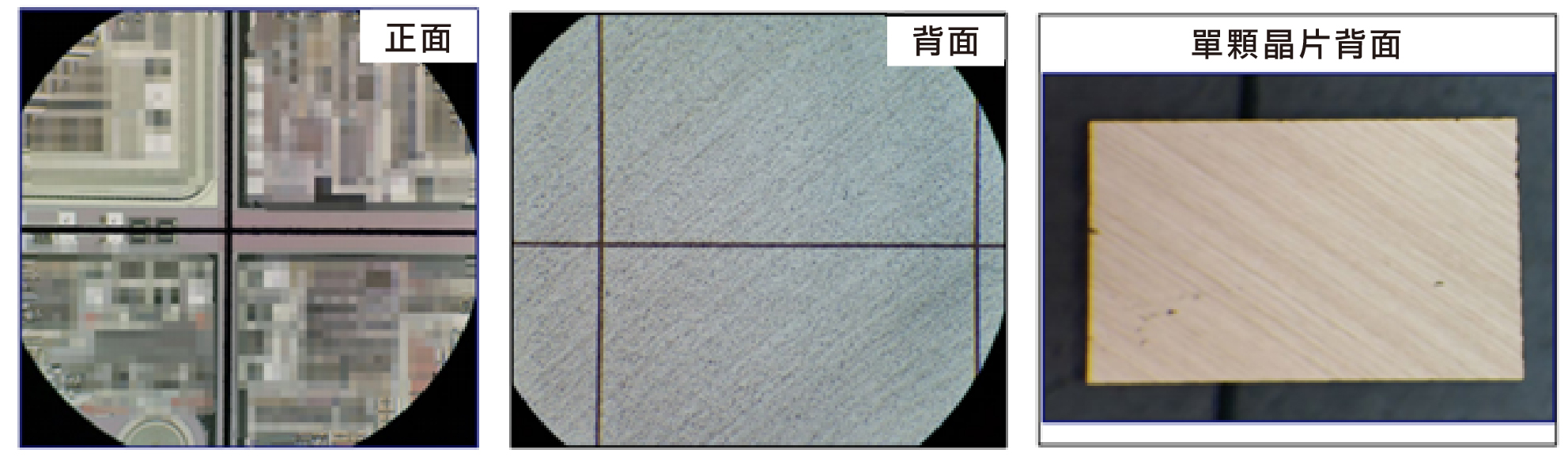
8-inch IC silicon wafer, cutting path contains metal, no laser burn.
Precautions:
- Check the Dicing Blade: Before installation, be sure to carefully inspect the dicing blade for cracks or chips. If damage is found, stop using it immediately to prevent danger.
- Confirm Rotation Direction: Ensure that the rotation direction mark on the dicing blade matches the actual rotation direction of the machine’s spindle. Using it in reverse will affect the cutting effect and blade life.
- Use the Correct Blade: Only use dicing blades that meet the specifications of the machine tool and processing conditions, avoiding processing failure or equipment damage due to non-compliant specifications.
- Immediate Shutdown: During the processing, if abnormal sounds, vibrations, or non-smooth cutting occurs, immediately stop the machine’s operation and find the cause before continuing.
- Regular Dressing: When you find that the cutting efficiency decreases, you should dress the blade. Continuing to use a dull blade may lead to overheating, overload, or even breakage.
- Do Not Touch: When the dicing blade is rotating, it is strictly forbidden to touch it with your hands or other body parts to avoid personal injury.
Any questions? Contact HonWay