
Over the past few decades, Moore’s Law has driven the rapid growth of the semiconductor industry, continuously improving chip performance and reducing costs through process miniaturization. However, as technology gradually approaches its physical limits, the traditional miniaturization strategy is facing a bottleneck—transistor sizes are nearing the atomic scale, and process difficulty and cost are rising sharply.
To overcome this dilemma, the semiconductor industry has begun to seek “heterogeneous integration” and “advanced packaging” as alternative paths to extend Moore’s Law. These technologies integrate chips of various processes, materials, and functions into a single package, not only enhancing performance but also reducing power consumption and shrinking size, driving applications like AI, high-performance computing, and the Internet of Things towards a new generation.
Table of Contents
Seven Key Values of Heterogeneous Integration and Advanced Packaging
As Moore’s Law gradually approaches its limits, traditional process miniaturization can no longer meet the demands for high-performance computing and multi-functional integration. Heterogeneous Integration and Advanced Packaging technologies have emerged, breaking through the limitations of single-chip design through methods such as chip stacking, including 2.5D, 3D packaging, and wafer-level packaging, to achieve system-level innovation. The following are seven key values that reveal the importance of this technology for the future development of semiconductors:
- Breaking the Limits of Moore’s Law: 3D stacking integrates multiple chips, breaking the bottleneck of traditional planar miniaturization.
- Improving Computing Performance: Shortens the signal path between chips, reducing latency and increasing bandwidth.
- Increasing Chip Density: Allows more logic and memory components to be housed within a package, supporting massive data processing.
- Lowering Power Consumption: Reduces the distance of electrical signal transmission, lowering energy consumption and heat dissipation pressure.
- Enabling Heterogeneous Integration: Integrates heterogeneous components such as CPUs, GPUs, memory, and sensors into a single module.
- Shrinking Product Size: Makes consumer electronics like wearables and smartphones smaller, thinner, and lighter.
- Enhancing Product Reliability: Improves system stability by refining packaging structures and reducing connection points.
Technological Evolution: The Ultimate Pursuit of “Flatness” and “Precision”
The success of both heterogeneous integration and advanced packaging hinges on the ultimate flatness and thickness consistency of wafer and chip surfaces. The following key packaging technologies have extremely strict requirements for surface conditions:
| Technology | Introduction | Surface Treatment Challenges |
| 3D IC | Stacking chips vertically and connecting layers via TSV | Chips must be highly flat to ensure vertical alignment and contact conductivity |
| Chiplet/small chip | Packaging multiple small chips side-by-side into a single module | The thickness of different chips must be extremely consistent to prevent package deformation or connection failure |
| Fan-Out | RDL (Redistribution Layer) technology to increase I/O density, often used for mobile SoC packaging | High requirements for the flatness of the chip edge and redistribution layer, which affects line formation and packaging quality |
| CoWoS / InFO | High-end 2.5D/3D packaging, applied in AI/HPC processors | The interface of chip and interposerneeds to be defect-free and precisely ground to the target thickness |
| TSV (Through-Silicon Via) | In the TSV process, holes must first be opened on the silicon wafer, followed by deposition, copper filling, and then CMP to remove excess metal and silicon layers, ensuring complete conduction and surface flatness. | To ensure through-hole conduction quality, the TSV CMP process requires a perfect balance between high selectivity, high uniformity, and extremely low damage |
CoWoS:Chip on Wafer on Substrate
What is Through-Silicon Via (TSV)?
In the pursuit of high-speed and high-density packaging for high-performance computing, smartphones, and AI chips, Through-Silicon Via (TSV) technology has become one of the core processes for realizing 3D ICs. Through vertical conductive holes, TSV can break the I/O limitations of traditional packaging, significantly shortening the distance between chips and the signal transmission path, improving electrical performance, and reducing power consumption.
The TSV process includes several highly precise steps:

- Depositing silicon dioxide (SiO₂) and photoresist on the silicon wafer surface.
- Using etching technology to open holes, forming via structures of a specific depth and diameter.
- Depositing a dielectric layer, a barrier layer, and a seed layer using Chemical Vapor Deposition (CVD) or Atomic Layer Deposition (ALD).
- Then, filling the holes with a highly conductive material, such as copper, and using Chemical Mechanical Planarization (CMP) to remove the excess metal layer to make the surface flat.
- Finally, using CMP again to remove the excess silicon layer, exposing the complete conductive vias to achieve vertical interconnection between multi-layer chips.
The TSV process has extremely high precision requirements not only for photolithography, deposition, and filling steps but also for back grinding, polishing, surface flatness, and metal residue control. To ensure the quality of through-hole conduction, the TSV CMP process needs to strike a perfect balance between high selectivity, high uniformity, and extremely low damage, which in turn presents greater challenges for grinding and polishing consumables.
Grinding and Polishing Consumables: The “Invisible Drivers” of Heterogeneous Integration and Advanced Packaging
In wafer processing and packaging workflows, grinding and polishing are not just about material removal but are core steps that determine packaging quality, performance, and yield. From chip backside grinding (backgrinding) and TSV fabrication to redistribution layer (RDL) processes, the choice of consumables will directly impact the integrity of microstructures and dimensional control.
Key Consumable Applications and Value
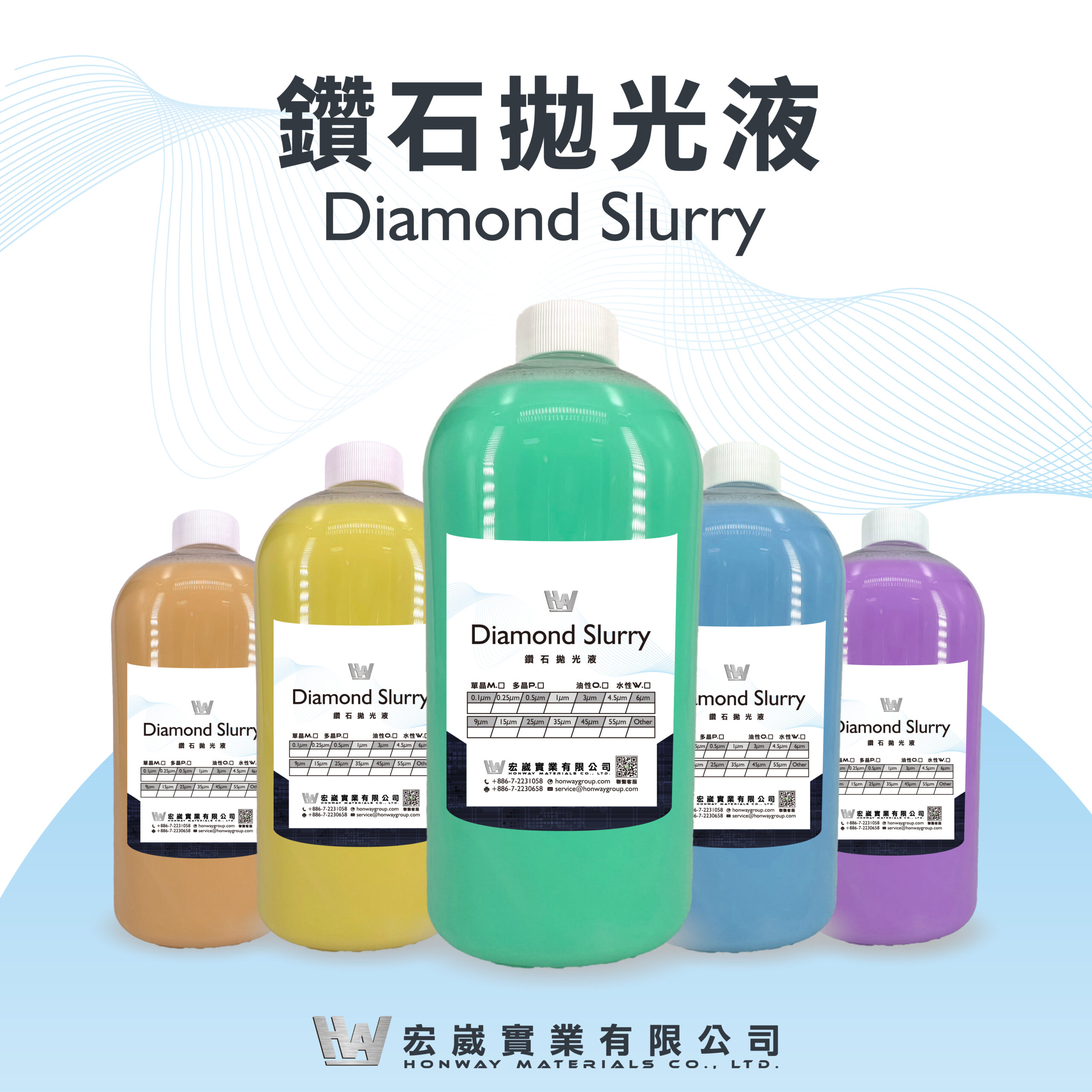
- Honway Diamond Polishing Liquid (Diamond Slurry): A powerful tool for high-hardness materials like SiC and GaN, featuring high efficiency and low scratch characteristics.
- CMP Polishing Pads and Polishing Liquid: Used for planarizing wafer surfaces or interposers, controlling Ra values and surface particle contamination.
- Wafer Grinding Wheels and Pads: For chip thinning and rough processing, emphasizing uniform pressure and stability.
- Honway Wafer Dicing Blade Series: Designed for various hard and brittle materials such as semiconductor wafers and packaging substrates, this series includes high-precision electroplated blades, stable and wear-resistant hard blades, and high-speed, long-life soft blades, comprehensively meeting the demands for high efficiency and high yield in wafer dicing and backend packaging.
Innovative Consumable Solutions: Breaking the Grinding and Polishing Bottlenecks of Advanced Packaging
As the pace of heterogeneous integration and advanced packaging accelerates, the challenges wafers face in critical stages like rough grinding, fine grinding, and Chemical Mechanical Planarization (CMP) are becoming increasingly severe. Honway Precision deeply understands that every micrometer of the process is crucial and has built a complete and efficient product line of grinding and polishing consumables tailored to different material characteristics and process needs, assisting customers in achieving higher yield and more stable output in high-end packaging technologies.
Honway polishing pad innovation: five-layer structure, comprehensively improving CMP performance
Honway’s polishing liquids utilize advanced nano-scale particle technology, offering various material-specific formulations and particle size options to achieve ultimate results for different surface characteristics:
| Item | STI, low-k dielectric layer | Silicon (Si) | Silicon Carbide (SiC) |
| Grinding Consumables | Cerium Oxide | Alumina, Silica Grinding Slurry/Powder | Diamond grinding slurry/paste |
| Grinding time | 20~30 minutes | 60~120 minutes | |
| Loss rate | <1% | ≧5~10% |
- Diamond Polishing Liquid: Honway’s diamond polishing liquid is designed for high-hardness materials like SiC and GaN. It utilizes surface microstructure modification technology, including the introduction of different structures such as spherical diamond particles, to effectively reduce scratches and surface stress during the grinding process, making the workpiece surface less susceptible to damage. This technology achieves extremely low sub-surface damage during the back grinding stage, providing a strong guarantee for the heat dissipation and reliability of high-power components.
- Aluminum Oxide Polishing Liquid: Effectively handles metal and silicon-based layers, balancing material removal rate with surface flatness, and is suitable for multi-layer stacking processes.
- Cerium Oxide Polishing Liquid: Exhibits excellent selectivity and low defect rates in STI and low-k materials, suitable for interlayer planarization in complex structures.
- Silicon Dioxide Polishing Liquid: Stable and highly uniform, providing an ideal fine polishing solution for advanced logic and memory processes.
Three Key Advantages:
- High Stability: Not prone to sedimentation or crystallization, effectively reducing process abnormality risks.
- Environmentally Friendly and Easy to Handle: Low toxicity and waste liquid-friendly design, in line with green manufacturing trends.
- Anti-Contamination Design: Low particle residue, bubbles, and surface contamination, ensuring minimized defect rates.
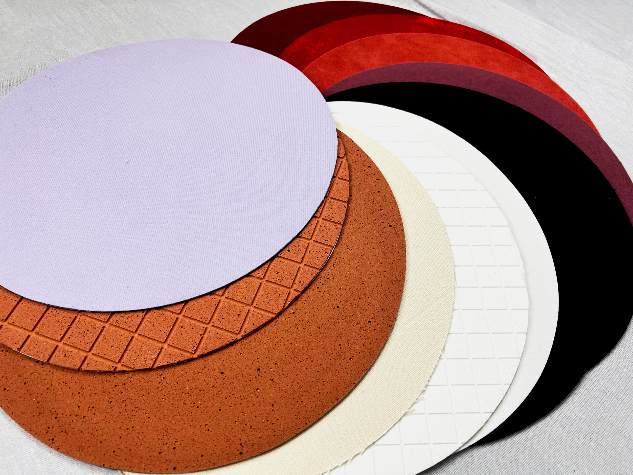
Honway’s Polishing Pad Innovation: Five-Layer Structure, Comprehensively Enhancing CMP Performance
As advanced semiconductor processes impose increasingly stringent requirements on surface quality, polishing pads, as critical consumables in the Chemical Mechanical Planarization (CMP) process, directly impact wafer surface roughness, material removal rate, and overall process stability. Honway’s precisely developed high-performance wafer grinding and polishing pads, combining innovative materials science with microstructure design, provide the industry with more efficient and cost-effective CMP solutions.
- Materials Science Breakthrough – Five-Layer Structure Achieves Functional Integration: Honway polishing pads feature a unique five-layer composite structure design. Compared to traditional single-layer or three-layer polishing pads, this design not only enhances mechanical strength and deformation control capabilities but also provides precise support and interface response for different process stages. Each layer has a clear division of labor, from rigid control of the carrier substrate, to elastic modulus and friction coefficient adjustment of the contact layer, and dynamic pressure adjustment capability of the surface layer. Each layer is precisely designed and material-optimized to ensure high matching with different types of polishing slurries (e.g., SiO₂, CeO₂, Al₂O₃, diamond, etc.), improving removal rate and surface uniformity.
- Microstructure Design – Smoother Slurry Flow and Bubble Release: Honway polishing pad surfaces are highly engineered with a high-density microporous structure and optimized groove patterns. This ensures uniform distribution of grinding fluid during polishing, preventing localized accumulation and dry friction, and effectively guiding bubble expulsion, reducing the risk of micro-scratches and surface defects.
- Long Lifespan and Process Stability: Honway polishing pads possess excellent wear resistance and shape retention. Even under long-term high-load conditions, they can maintain stable pressure distribution and grinding effect, significantly extending the pad’s service life. The extended replacement cycle not only reduces material costs but also minimizes downtime frequency and process variation risks, enhancing overall production line utilization and yield performance.
This design can effectively prevent dry friction, localized wear, and micro-scratches, and it supports and is compatible with multiple grinding liquids, such as cerium oxide, aluminum oxide, and diamond. Its wear resistance and extended lifespan not only improve process stability but also help reduce production costs and downtime risks.
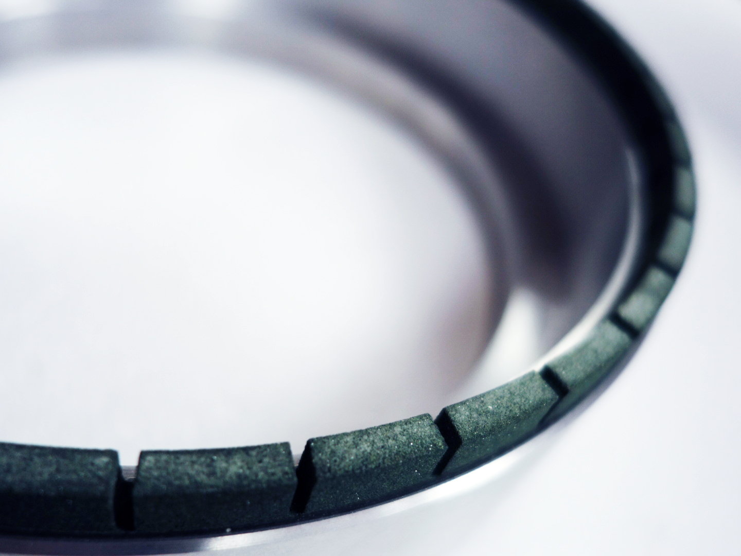
Honway Precision Grinding Wheel Series: High-Efficiency Solutions for Different Wafer Materials
To meet the strict requirements for roughness and surface quality at different stages of wafer processing, Honway offers a series of professional grinding wheels tailored to specific materials and applications:
- Chamfering and Grinding Wheels for Silicon Wafers
Used for wafer edge chamfering, effectively removing burrs and micro-cracks after cutting, ensuring smooth and damage-free edges, reducing the risk of wafer chipping due to micro-cracks in subsequent processes, and improving overall yield. - Grinding Wheels for Wafer Surface Grinding
Applied for silicon wafer surface planarization, Honway grinding wheels achieve an ideal balance of high removal rate and low surface roughness, helping wafers attain high flatness (TTV, WARP control) and low Ra values, which is an indispensable foundation for advanced packaging and high-end processes. - Grinding Wheels for Compound Semiconductors
In response to the increasingly widespread application of ultra-hard and brittle compound semiconductor materials like SiC and GaN, Honway has developed specialized high-hardness, high-wear-resistance grinding wheel formulations that can effectively achieve fast rough grinding while reducing surface micro-cracks and material damage, supporting the high-yield processing needs of power components and RF components.
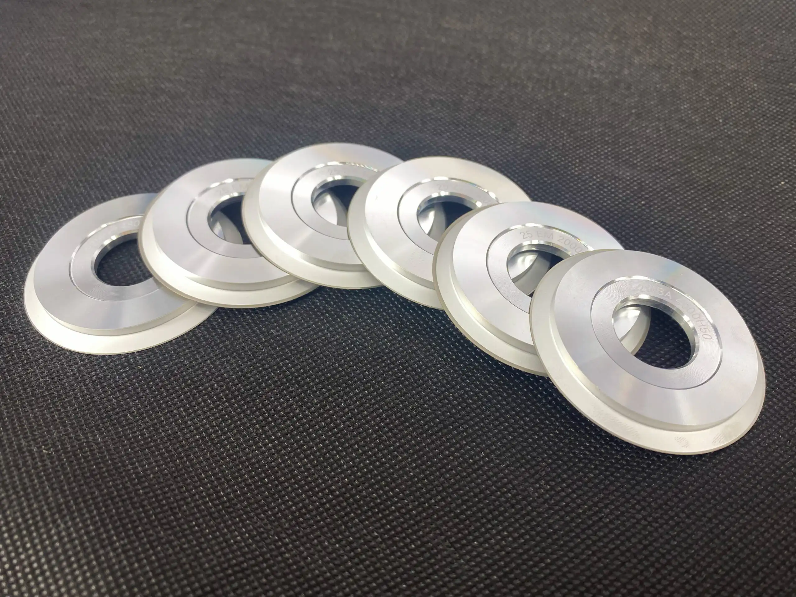
Honway Wafer Dicing Knife Series: Precise and Efficient Cutting Solutions for a Variety of Materials
To meet the high-precision and high-stability cutting demands for various hard and brittle materials in semiconductor assembly, testing, and backend packaging, Honway offers multiple professional dicing blade products, corresponding to different materials and application scenarios to ensure processing quality and process efficiency:
- Wafer Electroplated Dicing Blade
Suitable for silicon wafers, oxide wafers, and compound wafers such as SiC, GaAs, and GaP. It features an ultra-small kerf and high machining precision, effectively reducing cutting loss and improving die quality. It is widely used in wafer dicing and precision component processes. - Wafer Packaging Dicing Blade – Hard Blade
Made of a high-wear-resistant material with a stable blade structure, it can effectively control chip sidewall steps and dimensional accuracy. It is suitable for hard and brittle materials such as ceramic LED substrates, semiconductor packaging substrates, PZT, and TGG, serving as a stable and powerful tool for high-yield packaging processes. - 晶圓封裝划片刀-軟刀Wafer Packaging Dicing Blade – Soft Blade
With the dual advantages of high cutting speed (up to 200mm/s) and long lifespan (over 7000m), it is particularly suitable for high-efficiency mass production needs for materials such as PCBs, EMC, Chip LED substrates, and LTCC, PZT, and TGG, improving cutting efficiency and production stability.
Practicing the Future: Honway Technology’s Contribution to Heterogeneous Integration and Advanced Packaging
Facing the increasing complexity of the semiconductor industry, Honway Technology not only provides consumables but also offers complete solutions. Our strategies include:
- Forward-Looking R&D Investment: Honway actively collaborates with the advanced process supply chain, introducing customized formulations and nano-scale particle control technology.
- Precise Material Matching Capability: In response to complex multi-layer stacking structures and heterogeneous material integration, Honway provides consumable options with high selectivity and low defectivity.
- Proven Success Cases: Our diamond polishing liquid has been successfully applied in the wafer thinning stage for ultra-hard materials, achieving industry-leading surface roughness standards and endpoint control.
- Sustainable Manufacturing Orientation: All products use low-toxicity, easy-to-clean formulas, which are in line with green manufacturing trends and reduce customers’ environmental treatment costs.
Act now, and let’s together open a new chapter in semiconductor precision manufacturing!
- Free Consultation and Project Evaluation: Our Honway diamond industrial consumable experts provide product consultation and professional evaluation tailored to your specific process needs, working together to find the optimal grinding and polishing solution.
- Customized Solution Design: Whether you are facing challenges with silicon wafers or compound semiconductors (SiC, GaN, GaAs), we can customize the most suitable semiconductor grinding and polishing solutions for your needs.
- Advanced Materials and Performance Verification: We offer industry-leading Honway diamond polishing liquids, diamond disks, precision grinding wheels, and other consumables. We can also assist you with process implementation and performance verification to ensure your products achieve the expected high yield and excellent performance.
- Honway possesses stable supply capabilities, quality assurance, after-sales service, and customized support, ensuring the most consistent product quality for you.
Don’t let processing challenges limit your innovation! Contact us now, and let Honway’s diamond industrial consumables be your key to success!
More Information on Honway Diamond Grinding and Polishing Consumables:
To learn more about how Honway can bring breakthrough benefits to your semiconductor processes, please click the links below to explore our full range of diamond grinding and polishing consumables and technical details:
- Honway Nanodiamond Polishing Liquid Series
- Honway Precision Wafer Grinding and Polishing Pads
- Honway Grinding Wheels for Wafer Surface Grinding
- Honway Chamfering and Grinding Wheels for Silicon Wafers
- Honway Wafer Electroplated Dicing Blade
- Honway Wafer Packaging Dicing Blade – Soft Blade
- Honway Wafer Packaging Dicing Blade – Hard Blade
You can also directly “contact our Honway expert team,” and we will provide the most professional customized consultation and solutions.
Read More Related Topics
- Diamond Substrate>>>From jewelry to semiconductors: Diamonds play a key role in the next generation of thermal conductivity materials
- Compound Semiconductors>>>The secret weapon of semiconductor precision manufacturing: diamond grinding and polishing consumables, effectively improving wafer yield and performance!
- Semiconductor grinding and polishing>>>Grinding and Polishing in Semiconductor Manufacturing: Excellence from Material Selection to Consumable Empowerment
- Grinding and polishing cunsumbles>>>Innovative Grinding and Polishing Consumables: Driving the Semiconductor Industry Towards Higher Precision
- The key to ultra-flat wafers>>>The “Thin” Science of Semiconductor Grinding and Polishing: Key to Achieving Ultra-Flat Wafers
We offer customized adjustments to the grinding process, tailored to meet processing requirements for maximum efficiency.
After reading the content, if you still don’t know how to select the most suitable option,
Feel free to contact us and we will have specialist available to answer your questions.
If you need customized quotations, you’re also welcome to contact us.
Customer Service Hours: Monday to Friday 09:00~18:00 (GMT+8)
Phone: +8867 223 1058
If you have a subject that you want to know or a phone call that is not clear, you are welcome to send a private message to Facebook~~
Honway Facebook: https://www.facebook.com/honwaygroup
You may be interested in…
[wpb-random-posts]
(Source of the first image: shutterstock)