
In the global technology landscape, Taiwan is hailed as “Silicon Island,” not only for its powerful chip manufacturing capabilities but also for its pivotal role in the global semiconductor industry chain. But have you ever wondered, these core chips that power high-tech devices like smartphones, AI servers, and autonomous vehicles—their starting point is actually the sand beneath our feet?
Table of Contents
Where Does Silicon Come From? The Answer is on the Beach Beneath Your Feet
Silicon is the key material for manufacturing semiconductors, yet it doesn’t exist directly in nature. Instead, it is widely distributed in sand in the form of silicon dioxide (SiO₂). This gives the poetic phrase “a grain of sand, a world” concrete meaning in the semiconductor industry.
While ordinary sand also contains silicon, modern technology demands extremely high material purity. Therefore, the semiconductor industry generally uses a special raw material called “quartz sand” or “silica sand.” This sand comes from weathered granite and quartz vein minerals, with silicon content as high as 95%. It has not only minimal impurities but also physical properties more suitable for subsequent refining and crystal growth processes.
The Art of Crystal Refining: Quartz Sand → Metallurgical-Grade Silicon → Polysilicon
To transform silicon dioxide from quartz sand into usable silicon wafers requires three precise processes, an ultimate refinement that is a modern “art of crystal refining.”
- High-Temperature Reduction
The silicon and oxygen atoms in silicon dioxide are very tightly bonded and cannot be used directly. Therefore, in an electric arc furnace operating at over 1800°C, quartz sand reacts with carbon (such as coal or wood chips) to produce metallurgical-grade silicon (MG-Si) through a reduction reaction: SiO₂ + 2C → Si + 2CO↑, with a purity of 98–99%. Although this stage already allows for applications in industrial construction materials like alloys and building materials, it is still far from the high purity required for semiconductors. - Siemens Process Chemical Refining
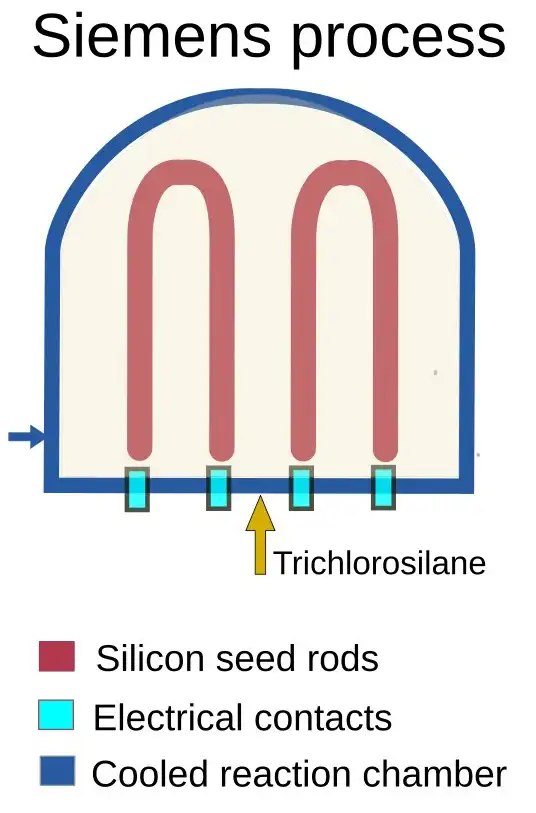
To further achieve a purity of over 99%, MG-Si needs to be chlorinated into trichlorosilane (SiHCl₃). Then, through the Siemens process (also known as Chemical Vapor Deposition, CVD), in a sealed bell-jar reactor, trichlorosilane is heated to approximately 1,100°C to vaporize it. Through a reduction reaction in the high-temperature environment, silicon elements are released from the gas and slowly deposited on heating rods or the inner surface of the furnace, gradually forming high-purity polysilicon with a stable crystalline structure and minimal impurities. This process can achieve an 11N等級(純度高達99.999999999%)11N grade (purity up to 99.999999999%) , this technology was developed by Siemens and Wacker in the 1950s and now accounts for more than 75-90% of the global electronic-grade polysilicon market share. The purity can reach electronic-grade 10N to 11N (99.999999999%), akin to refining dark sugar into ultra-clean white sugar.
Next, it enters the third process—the Czochralski process—to convert polysilicon into single-crystal silicon wafers.
Czochralski Process: Polysilicon → Single-Crystal Silicon Ingot
Having extremely high-purity polysilicon is only an intermediate step. Although high purity, polysilicon has an irregular appearance and an unordered internal structure. To become single-crystal silicon, which can be used in chip materials, it needs to be processed one more time. This critical process is called the Czochralski process.
The Czochralski Process, also known as the “crystal pulling method,” was invented by Polish scientist Jan Czochralski in 1916 and applied to semiconductor manufacturing in the 1950s. It remains the mainstream single-crystal silicon growth method today.
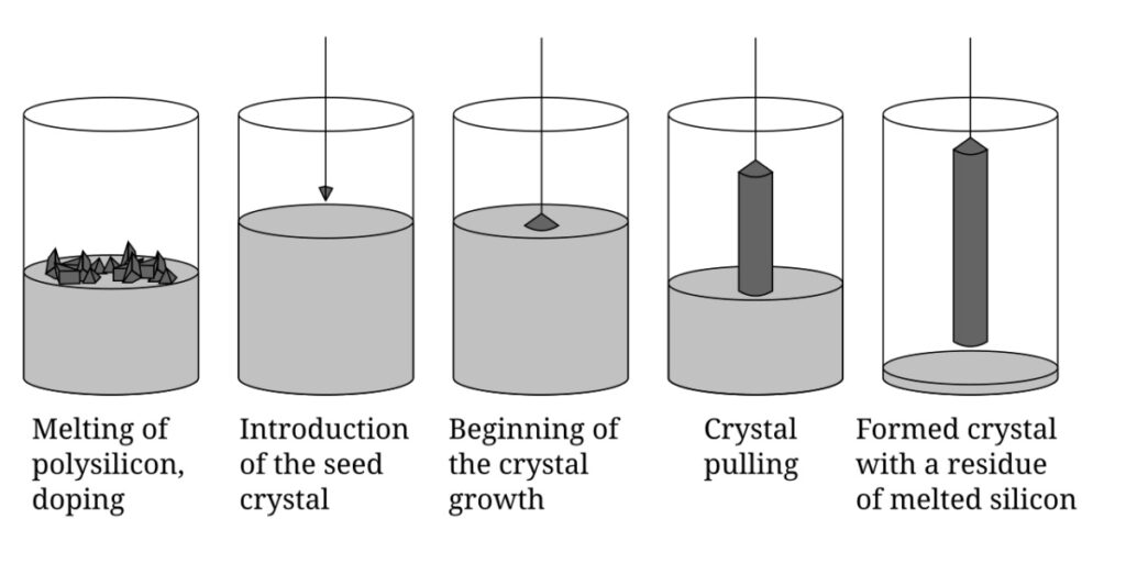
First, high-purity polysilicon is heated until completely molten and poured into a high-temperature resistant quartz crucible. Next, a “seed crystal rod” made of single-crystal silicon is vertically immersed into the molten silicon liquid, while precisely controlling the pulling and rotation speeds.
During this process, silicon atoms in the melt crystallize layer by layer, following the arrangement of the seed crystal, thereby growing into a single-crystal silicon ingot with a complete structure and no grain boundaries. This silicon ingot can reach a diameter of 30 cm and a length of over 1 meter, appearing like a “pulled sugar” made of silicon. The completed single-crystal silicon ingot is then sliced into thin, paper-like silicon wafers, each of which is the starting point for chip manufacturing and the foundational material for smart devices and high-end computing.
Behind the Wafer: Supporting the Entire AI and Digital World
Starting from seemingly inconspicuous grains of sand, through multiple stages of chemical reduction, gas purification, and high-temperature crystal pulling, each silicon wafer containing billions of transistors is ultimately produced. These wafers are the core of critical hardware like smart devices, servers, and autonomous vehicles, and they form the foundation of Taiwan’s technological competitiveness.
Every process not only embodies scientific precision but also represents the level of a country’s industrial chain integration capability. Taiwan is one of the few countries that holds a significant position in design, manufacturing, packaging, and application integration, making the name “Silicon Island” truly deserved.
Sustainability Challenges and Future Transformation
With global net-zero emission targets, the high energy consumption and emissions of the traditional Siemens process are being questioned. Emerging technologies like Molten Salt Electrolysis may break through technical bottlenecks, increasing crystalline silicon purity to 4-5N while reducing energy consumption by 90% and producing oxygen as a byproduct, making it a green alternative.
Additionally, methods such as FBR (Fluidized Bed Reactor) and zone refining, continuous melting, etc., are currently being experimented with, and are expected to bring more energy efficiency and environmental improvement benefits to the semiconductor and solar material fields in the future.
The Path of Silicon is Also the Path of Taiwan
In today’s surging era of AI, 5G, and high-performance computing, the global demand for high-quality silicon wafers continues to rise, and Taiwan already stands at the core of the supply chain. From sand to silicon wafers, this path is both a journey of material transformation and the best symbol of Taiwan’s technological strength.
Just as “a grain of sand, a world” suggests, every grain of sand holds infinite possibilities, and every wafer represents a story that changes the world. In this technological adventure, where the minuscule builds the magnificent, Taiwan is that Silicon Island blooming with prosperity.
(Source of the first picture: Getty Images/iStockphoto)
We offer customized adjustments to the grinding process, tailored to meet processing requirements for maximum efficiency.
Feel free to contact us and we will have specialist available to answer your questions.
If you need customized quotations, you’re also welcome to contact us.
Customer Service Hours: Monday to Friday 09:00~18:00 (GMT+8)
Phone: +8867 223 1058
If you have a subject that you want to know or a phone call that is not clear, you are welcome to send a private message to Facebook~~
Honway Facebook: https://www.facebook.com/honwaygroup
You may be interested in…
[wpb-random-posts]