
With the rapid growth of artificial intelligence, big data, and high-performance computing, data transmission technology is facing unprecedented challenges. While traditional electrical signals are widely used, their limitations in speed, latency, and energy consumption are gradually becoming insufficient for modern computing demands. Silicon photonics technology has therefore become one of the global technology fields’ focal points. Recently, China’s Fudan University announced the successful development of a multiplexer chip that uses light as the signal transmission medium, demonstrating the potential of light-based data processing in terms of speed and efficiency, and triggering widespread discussion about the application prospects of photonics chips. This new development may bring new thinking to future chip architectures and data centers.
Table of Contents
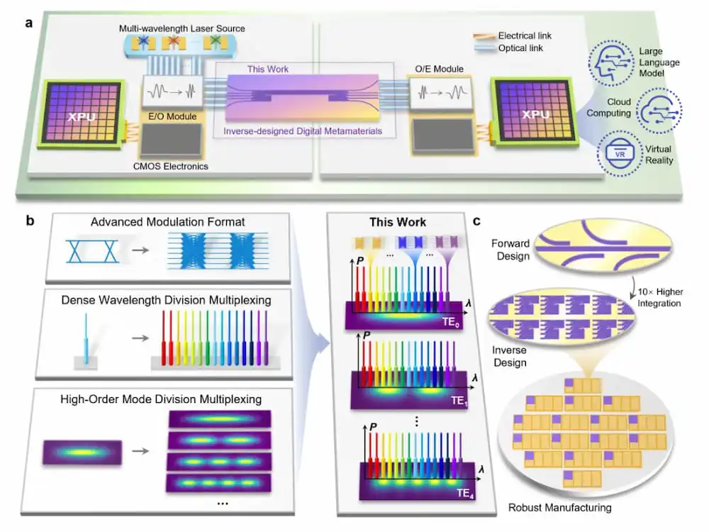
Light Signals Replace Electrical Signals: A Fundamental Innovation in Transmission Methods
As artificial intelligence and high-performance computing technologies develop rapidly, traditional electrical signal transmission methods are gradually facing limitations in speed and energy consumption. To overcome these bottlenecks, the scientific community is actively researching new methods that use light signals to replace electrical signals. Silicon photonics technology is rapidly emerging against this backdrop, with its core lying in using light to transmit data and instructions, which is expected to significantly improve computing performance and reduce latency.
Fudan University in China recently announced the development of a “silicon photonics integrated higher-order mode multiplexer chip,” capable of ultra-high-speed optical signal processing. This is regarded as a significant step towards the practical application of photonics chips. The technology has been submitted to an international journal, demonstrating its potential at both academic and technical levels.
Multiplexer Technology: Key to Supporting High-Speed Data Flow
The core of this new chip is a component called a multiplexer. A multiplexer can select signals from multiple data sources and transmit them via a single path, making it a crucial component for handling high-speed, high-volume data flow. Fudan University’s tests show that this silicon photonics multiplexer has a transmission rate of up to 38 Tbps. Theoretically, it can transmit approximately 4.75 trillion parameters of large language models per second, which holds substantial application value for the ever-expanding scale of AI models.
This advancement helps address the bandwidth challenges currently faced by large model training, especially in data centers and high-performance servers, where high-speed connections between chips have become one of the bottlenecks for system performance.
Optoelectronic Integration: Overcoming Communication Barriers Between Heterogeneous Systems
While silicon photonics chips show impressive performance, achieving their integration with existing electronic component systems remains a critical technical challenge. Currently, most memory and logic systems still rely on CMOS electronic architectures. How to seamlessly connect optical and electrical signals is a technical hurdle for promoting optoelectronic convergence.
One of the key aspects of Fudan University’s technology is the chip’s ability to integrate light-based transmission with CMOS architecture in a low-latency manner, allowing photonic and electronic components to work collaboratively on the same platform. This has forward-looking significance for building new-generation high-performance hybrid architecture processors in the future.
Modal Multiplexing Design: Enhancing Bandwidth and Transmission Efficiency
Compared to traditional single-mode communication architectures, this chip adopts higher-order modal multiplexing technology, enabling simultaneous transmission of multiple independent optical data paths, significantly increasing bandwidth density and communication efficiency. This design not only improves the chip’s data processing capability per unit area but also helps reduce the number of transmission channels required by the system.
Relevant technological observations indicate that this architectural breakthrough is a response to the current demand for high-speed, low-latency data exchange in artificial intelligence applications. With the continuous expansion of model scales, photonic data communication may become the mainstream direction for future system architecture design.
(Image source: Chinese Media)
Commercial Potential and Implementation Challenges Coexist
Although the chip is currently in the experimental stage, some views suggest that related technologies are expected to achieve application-level breakthroughs within three to five years. Particularly in fields such as large model training, parallel computing, and internal data center communication, photonic chips have the potential to improve system performance and reduce energy consumption.
However, moving from prototype chips to large-scale mass production still requires overcoming numerous technical and cost challenges, including the process stability of photonic components, compatibility with existing silicon-based manufacturing lines, and optimization of overall packaging and thermal management technologies. Researchers emphasize that the chip is still an early result, and its stability and scalability need further verification in subsequent work.
Global Perspective: The Photonics Technology Race
In recent years, multiple countries worldwide have actively invested in the research and development of photonics technology, and China’s performance in this area has also received increasing attention. According to statistics, in the field of chip research in the “post-Moore era,” China’s academic paper output is already among the global leaders, with a significant growth in citations and technical patents, especially in photonics-related fields.
This reflects China’s attempt to seek a leading position in emerging architectural fields through technological innovation. Some observers suggest that within the next decade, China may narrow or even surpass the gap with some traditional technological powerhouses in cutting-edge areas like silicon photonics.
Conclusion
The silicon photonics multiplexer chip launched by Fudan University is undoubtedly a significant achievement in global photonics technology development. Although it is currently in the experimental stage, its demonstrated technological potential is enough to inspire more imagination about the future transformation of information transmission modes.
The realization of optoelectronic integration, the reconstruction of system architecture, and the feasibility of large-scale deployment are all key aspects driving the practical application of photonics chips. In the next few years, whether this technology can move from laboratories into data centers and computing platforms will be a key observation point for the successful industrialization of silicon photonics.
References:
- Transmission Speed Reaches 38Tbps! China’s Silicon Photonics Chip Emerges, Major Breakthrough Expected Within Three Years?
- Chinese researchers invent silicon photonic multiplexer chip that uses light instead of electricity for communication — CCP says China’s early steps into light-based chips precede ‘major breakthroughs’ in three years
- Chinese researchers develop ultra-high-capacity chip, facilitating on-chip optical data transmission
(Source of the first picture: VCG)
We offer customized adjustments to the grinding process, tailored to meet processing requirements for maximum efficiency.
Feel free to contact us and we will have specialist available to answer your questions.
If you need customized quotations, you’re also welcome to contact us.
Customer Service Hours: Monday to Friday 09:00~18:00 (GMT+8)
Phone: +8867 223 1058
If you have a subject that you want to know or a phone call that is not clear, you are welcome to send a private message to Facebook~~
Honway Facebook: https://www.facebook.com/honwaygroup
You may be interested in…
[wpb-random-posts]