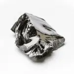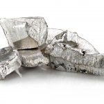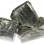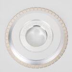
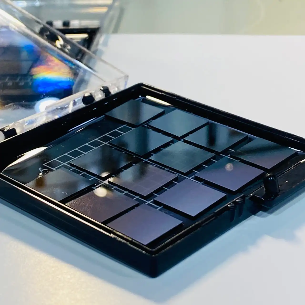
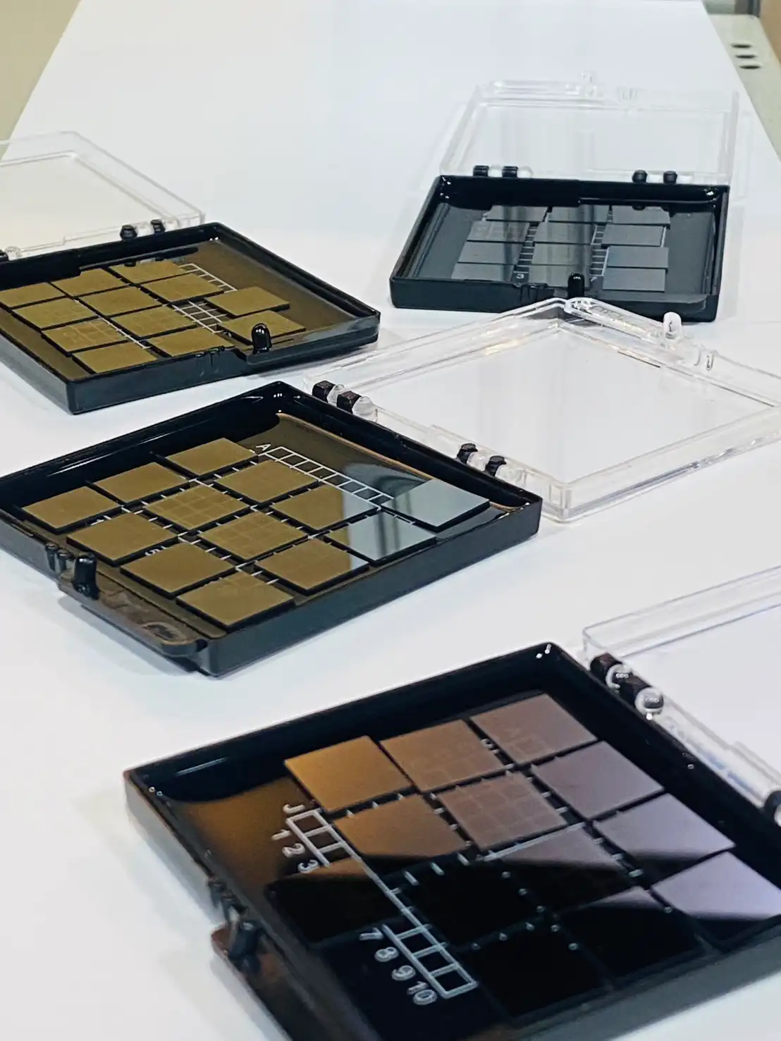
Diamond Substrate/Diamond Wafer
Diamond Substrate/Diamond Wafer
Honway Materials provide customized services,
Manufacturing the most suitable diamond substrate/diamond wafer for you.
Product Features:
- CVD diamond is manufactured using the Chemical Vapor Deposition method.
- Diamond possesses the highest thermal conductivity among all known materials, enabling effective and rapid heat dissipation.
- Possesses excellent wear resistance and damage resistance. Suitable for various high-durability applications, including precision cutting tools, industrial saw blades, and drilling equipment.
- Exhibits high transparency and low absorption across a broad wavelength range, making it an ideal material for optical windows, lenses, and high-performance optical components.
- Highly resistant to corrosion from acids, alkalis, and most chemical substances, maintaining stable performance for extended periods even in harsh chemical environments.
- Non-toxic and does not cause rejection reactions with human tissues, widely used in medical devices and implantable devices.
Application areas:
-
Thermal Interface Materials (TIMs): Diamond wafers can be used as high-efficiency thermal interface materials between chips, modules, and heat sinks, effectively reducing thermal resistance, significantly improving thermal conductivity efficiency, and ensuring stable equipment operation.
-
Electronic Packaging and Substrates: In the semiconductor packaging field, diamond wafers provide excellent heat dissipation performance, supporting continuous operation of components in high power density environments, further promoting the miniaturization and high performance of electronic products.
- Server Applications: Can serve as an ideal heat spreader for high-power components such as GaN or SiC crystals, effectively reducing internal temperature rise, extending component lifespan, and improving system reliability. In addition, its excellent mechanical strength and high-temperature resistance are also very suitable for advanced packaging technologies such as 2.5D/3D stacking and high-performance computing platforms in data centers.
-
LED and Optoelectronic Components: Applied in fields such as LEDs and optoelectronic components, diamond wafers can significantly improve thermal management, extend component lifespan, and enhance luminous brightness and energy efficiency, meeting the demands of high-end optoelectronic applications.
-
Insulation Substrates: CVD diamond wafers are used as insulation substrates for high-performance semiconductors. Their electrical insulation and high thermal conductivity make them ideal for power devices and RF (radio frequency) components.
- Medical Devices: Industrial-grade diamonds are also used in some medical fields, such as high-precision surgical instruments and dental drills. Due to diamond’s high hardness and wear resistance, it can improve the service life and accuracy of medical devices.
Product Specification:
| Grade | Optical Grade | Heat sink grade |
| Diamond Type | Monocrystalline | Polycrystalline |
| Wafer size | Maximum 15*15mm², customizable | 2 inches, customizable |
| Grit size | ≤10μm | |
| Diameter tolerance | ﹢0.1, -0mm | ﹢0.1, -0mm |
| Thickness | 0.3-1.5mm | |
| Thickness after polishing | 0.1~2mm | 0.2-1.0mm |
| Thickness tolerance | ±0.02mm≤10mm
±0.03mm, 10~15mm |
±50μm |
| Crystallographic direction | 100 | |
| Surfaece treatment- | Polishing, Ra<2nm | |
| Growth surface roughness | <100nm Ra | |
| Nucleation surface roughness | <30nm Ra | |
| Standard thickness | 300μm |
※ If you have any customized needs, please contact Honway
Physical Properties:
| Grade | Optical Grade | Heat sink grade |
| Diamond Type | Monocrystalline | Polycrystalline |
| Density | 3.52 g/cm3 | 3.52 g/cm3 |
| Raman full width at half maximum (FWHM) | ~2.1 cm⁻¹ | |
| Nitrogen concentration | <0.5 ppm | |
| Thermal conductivity | 1900~2200 W/(m·K) 300K | 1200~2000 W/(m·K) 300K |
| Transmittance | >70% 1064 nm | |
| Refractive Index | 2.379 @ 10.6 um | |
| Young’s modulus | 850GPa | |
| Chemical stability | Insoluble in all acids and bases | |
| Breaking strength | 350GPa | |
| Parallelism | <4μm/cm |
Diamond Specifications Comparison:
|
Monocrystalline CVD Diamond Wafer |
Polycrystalline CVD Diamond Wafer |
|
| Structure | Single, continuous crystal structure | Multiple randomly oriented small crystals |
| Mechanical properties | Excellent hardness, strength and wear resistance | Low strength, affected by grain boundaries |
| Thermal conductivity | Higher, excellent heat dissipation performance | Lower (due to grain boundaries) |
| Optical properties | Exceptional optical clarity and precision | Low clarity, may have flaws |
| Electrical properties | Highly controllable, direction dependent | High isotropy, low controllability |
| Application | Electronics, optics, high performance applications | Industrial tools, radiators, abrasives, heat dissipation materials |
Performance comparison of diamond and other common infrared materials:
| Physical Properties | Unit | Diamond | ZnSe | ZnS | Ge | Si | GaAs | Al₂O₃ | |
| Band gap | eV | 5.48 | 2.7 | 3.9 | 0.664 | 1.11 | 1.42 | 9.9 | |
| Cut-off wavelength | μm | 20 | 14 | 23 | 5.5 | ||||
| Absorption coefficient | 0.1~0.3 | 0.005 | 0.2 | 0.02 | 0.35 | 0.01 | |||
| Absorption coefficient | 10.6 μm | 0.1~0.6 | 0.0005 | 0.2 | 0.02 | ||||
| Microhardness | kg/mm² | 8300 | 137 | 230 | 780 | 1150 | 721 | 190 | |
| Refractive index | 2.38 | 2.40 | 2.19 | 4.00 | 3.42 | 3.28 | 1.63 | ||
| dn/dT | 10⁻³/K | 1.0 | 6.4 | 4.1 | 40 | 13 | 15 | 1.3 | |
| Thermal conductivity | W/(cm·K) | 18~22 | 0.19 | 0.27 | 0.59 | 1.63 | 0.55 | 0.35 | |
| Coefficient of thermal expansion | 10⁻⁶K⁻¹ | Optical Grade | 1.3 | 7.6 | 7.9 | 5.9 | 2.56 | 5.9 | 5.8 |
| Heat sink grade | 0.8~1.0 | ||||||||
Any questions? Contact HonWay